- Career Paths
- Diversity, Equity, and Inclusion
- DMSE Job Opportunities
- Our Faculty
- Computing and Data Science
- Energy and the Environment
- Health and Medicine
- Manufacturing
- Transportation and Infrastructure
- Archaeological Materials
- Semiconductors
- Soft Matter
- Characterization
- Computation and Design

Device Fabrication
- Synthesis and Processing
- Impact Stories
- Research Facilities
- Majors, Minors, and Concentration
- Opportunities For First-Year Students
- Opportunities for DMSE Undergraduates
- DMSE Breakerspace
- Wulff Lecture
- Application Assistance and Resources
- Doctoral Degree and Requirements
- Master’s Degree and Requirements
- Interdisciplinary Graduate Programs
- Funding Opportunities
- Postdoctoral Program
- MITx Online
- Newsletter Archive
- FORGE Initiative
Putting it All Together
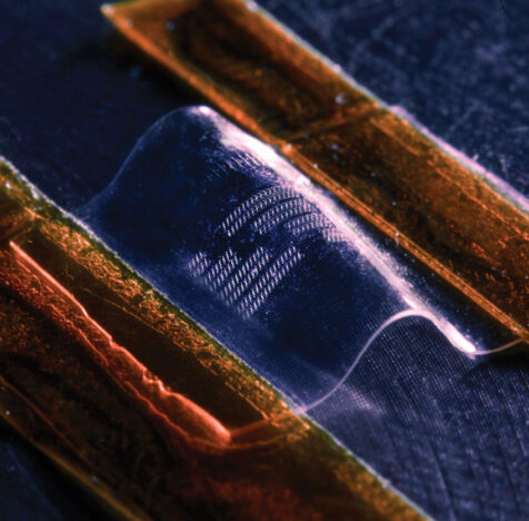
In materials science and engineering, device fabrication is the process of assembling discrete materials into a functional form. Materials scientists and engineers build devices, such as electronic or optical devices, with tailored properties that can be used for a range of applications, including information technology, renewable energy, and medical treatment.
The steps involved in device fabrication can vary depending on the type of device being developed and the materials used. For example, the fabrication process for a solar cell may involve the layering of thin films of photovoltaic materials onto a surface; producing a semiconductor device may involve the use of lithography to etch a silicon wafer.
Device Fabrication at DMSE
DMSE researchers make all kinds of devices. They’re developing new materials and processes for fabricating more efficient solar cells and devices for storing energy such as solar cells and batteries. Research teams are assembling electronics components such as diodes and transistors, including a rechargeable battery in the form of a fiber that can be woven into fabrics. And for health and medicine, they’re fashioning fibers from polymers and composite materials that can deliver drugs to the brain.
Related Materials
Related faculty and researchers.

Key Publications
Significantly enhanced sub-ambient passive cooling enabled by evaporation, radiation, and insulation, what we did.
Achieved substantial cooling capacity by controlling the effects of evaporative cooling, radiation, and thermal transport. Even in high-humidity areas, the process works without electricity and needs very little water.
Why we did it
Why it matters, reconfigurable all-dielectric metalens with diffraction-limited performance.
Proved that you don’t need mechanical movement to change the focus of a lens. Instead, a transparent “metalens” changes the way it interacts with infrared light when it undergoes heat-based phase transformation. To see objects far and near, one would simply heat the material using microheaters.
Thank you for visiting nature.com. You are using a browser version with limited support for CSS. To obtain the best experience, we recommend you use a more up to date browser (or turn off compatibility mode in Internet Explorer). In the meantime, to ensure continued support, we are displaying the site without styles and JavaScript.
- View all journals
- Explore content
- About the journal
- Publish with us
- Sign up for alerts
- Perspective
- Published: 19 June 2023
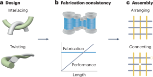
Design, fabrication and assembly considerations for electronic systems made of fibre devices
- Kaiwen Zeng 1 na1 ,
- Xiang Shi 1 na1 ,
- Chengqiang Tang 1 na1 ,
- Ting Liu 2 &
- Huisheng Peng ORCID: orcid.org/0000-0002-2142-2945 1
Nature Reviews Materials volume 8 , pages 552–561 ( 2023 ) Cite this article
4989 Accesses
12 Citations
4 Altmetric
Metrics details
- Electronic devices
- Electronic materials
Fibre electronic devices with one-dimensional configurations have attracted increasing interest because they are highly flexible and can be deformed. In particular, they can be woven into breathable and comfortable textiles for wearable applications. Fibre devices with various functionalities, such as energy harvesting and storage, sensing, and display, have thus been extensively explored. However, most fibre devices work individually rather than as systems. This Perspective aims to highlight promising design concepts, assembly strategies and performance improvements for fibre electronic systems. Their real-life applications are then analysed from a multidisciplinary point of view involving materials science, electrical engineering, textile engineering and health monitoring. The remaining challenges are finally summarized to guide future research for both academia and industry.
This is a preview of subscription content, access via your institution
Access options
Access Nature and 54 other Nature Portfolio journals
Get Nature+, our best-value online-access subscription
24,99 € / 30 days
cancel any time
Subscribe to this journal
Receive 12 digital issues and online access to articles
111,21 € per year
only 9,27 € per issue
Buy this article
- Purchase on Springer Link
- Instant access to full article PDF
Prices may be subject to local taxes which are calculated during checkout
High-quality semiconductor fibres via mechanical design

Integration of multiple electronic components on a microfibre towards an emerging electronic textile platform

Design and fabrication of wearable electronic textiles using twisted fiber-based threads
Xu, X., Xie, S., Zhang, Y. & Peng, H. The rise of fiber electronics. Angew. Chem. Int. Ed. 58 , 13643–13653 (2019).
CAS Google Scholar
Heo, J. S., Eom, J., Kim, Y. H. & Park, S. K. Recent progress of textile-based wearable electronics: a comprehensive review of materials, devices, and applications. Small 14 , 1703034 (2018).
Google Scholar
Zeng, W. et al. Fiber-based wearable electronics: a review of materials, fabrication, devices, and applications. Adv. Mater. 26 , 5310–5336 (2014).
Fakharuddin, A. et al. Fiber-shaped electronic devices. Adv. Energy Mater. 11 , 2101443 (2021).
Liu, R., Wang, Z. L., Fukuda, K. & Someya, T. Flexible self-charging power sources. Nat. Rev. Mater. 7 , 870–886 (2022).
Chen, C. et al. Functional fiber materials to smart fiber devices. Chem. Rev. 123 , 613–662 (2023).
Chen, G. et al. Electronic textiles for wearable point-of-care systems. Chem. Rev. 122 , 3259–3291 (2022).
Libanori, A., Chen, G., Zhao, X., Zhou, Y. & Chen, J. Smart textiles for personalized healthcare. Nat. Electron. 5 , 142–156 (2022).
Wang, L. et al. Application challenges in fiber and textile electronics. Adv. Mater. 32 , 1901971 (2020).
Ates, H. C. et al. End-to-end design of wearable sensors. Nat. Rev. Mater. 7 , 887–907 (2022).
Zheng, Y. Q. et al. Monolithic optical microlithography of high-density elastic circuits. Science 373 , 88–94 (2021).
Dong, K. et al. Advances in high-performance autonomous energy and self-powered sensing textiles with novel 3D fabric structures. Adv. Mater. 34 , 2109355 (2022).
Wang, Y., Yokota, T. & Someya, T. Electrospun nanofiber-based soft electronics. npg Asia Mater. 13 , 22 (2021).
Peng, H. Fiber electronics. Adv. Mater. 32 , 1904697 (2020).
Xu, Y. et al. A one-dimensional fluidic nanogenerator with a high power conversion efficiency. Angew. Chem. Int. Ed. 56 , 12940–12945 (2017).
Liu, P. et al. Polymer solar cell textiles with interlaced cathode and anode fibers. J. Mater. Chem. A 6 , 19947–19953 (2018).
Chen, C. et al. Direct current fabric triboelectric nanogenerator for biomotion energy harvesting. ACS Nano 14 , 4585–4594 (2020).
Liao, M., Ye, L., Zhang, Y., Chen, T. & Peng, H. The recent advance in fiber-shaped energy storage devices. Adv. Electron. Mater. 5 , 1800456 (2019).
Wang, L. et al. Functionalized helical fibre bundles of carbon nanotubes as electrochemical sensors for long-term in vivo monitoring of multiple disease biomarkers. Nat. Biomed. Eng. 4 , 159–171 (2020).
Shi, X. et al. Large-area display textiles integrated with functional systems. Nature 591 , 240–245 (2021).
Choi, H. W. et al. Smart textile lighting/display system with multifunctional fibre devices for large scale smart home and IoT applications. Nat. Commun. 13 , 814 (2022).
He, J. et al. Scalable production of high-performing woven lithium-ion fibre batteries. Nature 597 , 57–63 (2021).
Seyedin, S. et al. Fibre electronics: towards scaled-up manufacturing of integrated e-textile systems. Nanoscale 13 , 12818–12847 (2021).
Zhao, X. et al. Soft fibers with magnetoelasticity for wearable electronics. Nat. Commun. 12 , 6755 (2021).
AMERI Research. Smart textiles market to 2024: key product categories (active, passive, ultra smart), application (sensing, thermo-electricity, energy harvesting, luminescence & aesthetics), end-use, regional segmentation, competitive dynamics, M&A insights, pricing analysis (OPP, IPP, RAP) and segment forecast. AMERI Research https://www.ameriresearch.com/product/smart-textiles-market/ (2017).
Sun, H., Zhang, Y., Zhang, J., Sun, X. & Peng, H. Energy harvesting and storage in 1D devices. Nat. Rev. Mater. 2 , 17023 (2017).
Khudiyev, T. et al. Thermally drawn rechargeable battery fiber enables pervasive power. Mater. Today 52 , 80–89 (2022).
Liao, M. et al. Industrial scale production of fibre batteries by a solution-extrusion method. Nat. Nanotechnol. 17 , 372–377 (2022).
Zhang, Y., Wang, H., Lu, H., Li, S. & Zhang, Y. Electronic fibers and textiles: recent progress and perspective. iScience 24 , 102716 (2021).
Agcayazi, T., Chatterjee, K., Bozkurt, A. & Ghosh, T. K. Flexible interconnects for electronic textiles. Adv. Mater. Technol. 3 , 1700277 (2018).
Castano, L. M. & Flatau, A. B. Smart fabric sensors and e-textile technologies: a review. Smart Mater. Struct. 23 , 053001 (2014).
Loke, G. et al. Digital electronics in fibres enable fabric-based machine-learning inference. Nat. Commun. 12 , 3317 (2021).
Rein, M. et al. Diode fibres for fabric-based optical communications. Nature 560 , 214–218 (2018).
Zhang, Z. et al. A one-dimensional soft and color-programmable light-emitting device. J. Mater. Chem. C 6 , 1328–1333 (2018).
Zhang, Z. et al. Textile display for electronic and brain-interfaced communications. Adv. Mater. 30 , 1800323 (2018).
Zhang, Z. et al. A colour-tunable, weavable fibre-shaped polymer light-emitting electrochemical cell. Nat. Photon. 9 , 233–238 (2015).
Ye, L. et al. Stabilizing lithium into cross-stacked nanotube sheets with an ultra-high specific capacity for lithium oxygen batteries. Angew. Chem. Int. Ed. 58 , 2437–2442 (2019).
Chen, J. Y. et al. Electrospun poly(3-hexylthiophene) nanofibers with highly extended and oriented chains through secondary electric field for high-performance field-effect transistors. Adv. Electron. Mater. 1 , 1400028 (2015).
Yang, Q. et al. In situ formation of Co 9 S 8 quantum dots in MOF-derived ternary metal layered double hydroxide nanoarrays for high-performance hybrid supercapacitors. Adv. Energy Mater. 10 , 1903193 (2020).
Fu, X., Xu, L., Li, J., Sun, X. & Peng, H. Flexible solar cells based on carbon nanomaterials. Carbon 139 , 1063–1073 (2018).
Hu, Y. et al. Photo-to-electricity generation of aligned carbon nanotubes in water. J. Mater. Chem. A 7 , 1996–2001 (2019).
Gao, Z. et al. Flexible self-powered textile formed by bridging photoactive and electrochemically active fiber electrodes. J. Mater. Chem. A 7 , 14447–14454 (2019).
Nakanishi, Y. et al. Concentrated-polymer-brush-modified silica nanoparticles self-assembled in ionic liquid containing iodide/tTriiodide (I – /I 3 – )-redox system as quasi-solid electrolytes for dye-sensitized solar cells. ACS Appl. Nano Mater. 4 , 6620–6628 (2021).
Liu, Y. et al. Electron-affinity-triggered variations on the optical and electrical properties of dye molecules enabling highly efficient dye-sensitized solar cells. Angew. Chem. Int. Ed. 57 , 14125–14128 (2018).
Xie, X., Criddle, C. & Cui, Y. Design and fabrication of bioelectrodes for microbial bioelectrochemical systems. Energy Environ. Sci. 8 , 3418–3441 (2015).
Pereira, A. R., de Souza, J. C. P., Iost, R. M., Sales, F. C. P. F. & Crespilho, F. N. Application of carbon fibers to flexible enzyme electrodes. J. Electroanal. Chem. 780 , 396–406 (2016).
Khudiyev, T. et al. 100 m long thermally drawn supercapacitor fibers with applications to 3D printing and textiles. Adv. Mater. 32 , 2004971 (2020).
Hong, S. et al. Carbon nanotube fibers with high specific electrical conductivity: synergistic effect of heteroatom doping and densification. Carbon 184 , 207–213 (2021).
Zhang, X., Lu, W., Zhou, G. & Li, Q. Understanding the mechanical and conductive properties of carbon nanotube fibers for smart electronics. Adv. Mater. 32 , 1902028 (2020).
Shen, B., Zhai, W. & Zheng, W. Ultrathin flexible graphene film: an excellent thermal conducting material with efficient EMI shielding. Adv. Funct. Mater. 24 , 4542–4548 (2014).
Fang, B., Chang, D., Xu, Z. & Gao, C. A review on graphene fibers: expectations, advances, and prospects. Adv. Mater. 32 , 1902664 (2020).
Zhang, R. et al. Growth of half-meter long carbon nanotubes based on Schulz–Flory distribution. ACS Nano 7 , 6156–6161 (2013).
Zhang, R., Zhang, Y. & Wei, F. Controlled synthesis of ultralong carbon nanotubes with perfect structures and extraordinary properties. Acc. Chem. Res. 50 , 179–189 (2017).
Ren, J., Sun, X., Chen, P., Wang, Y. & Peng, H. Research progress of fiber-shaped electrochemical energy storage devices. Chin. Sci. Bull. 65 , 3150–3159 (2020).
Lim, H.-R. et al. Advanced soft materials, sensor integrations, and applications of wearable flexible hybrid electronics in healthcare, energy, and environment. Adv. Mater. 32 , 1901924 (2020).
Jain, R. et al. Nanostructuring versus microstructuring in battery electrodes. Nat. Rev. Mater. 7 , 736–746 (2022).
Liu, X. H. et al. Size-dependent fracture of silicon nanoparticles during lithiation. ACS Nano 6 , 1522–1531 (2012).
Yan, W. et al. Single fibre enables acoustic fabrics via nanometre-scale vibrations. Nature 603 , 616–623 (2022).
Zeng, S. et al. Hierarchical-morphology metafabric for scalable passive daytime radiative cooling. Science 373 , 692–696 (2021).
Wang, Y. et al. 3D-printed all-fiber Li-ion battery toward wearable energy storage. Adv. Funct. Mater. 27 , 1703140 (2017).
Fu, K. et al. Graphene oxide-based electrode inks for 3D-printed lithium-ion batteries. Adv. Mater. 28 , 2587–2594 (2016).
Li, Y. et al. 3D-printed, all-in-one evaporator for high-efficiency solar steam generation under 1 sun illumination. Adv. Mater. 29 , 1700981 (2017).
Kaufman, J. J. et al. Structured spheres generated by an in-fibre fluid instability. Nature 487 , 463–467 (2012).
Kanik, M. et al. Strain-programmable fiber-based artificial muscle. Science 365 , 145–150 (2019).
Shen, Y. et al. Thermally drawn multifunctional fibers: toward the next generation of information technology. InfoMat 4 , e12318 (2022).
Fuller, B. J. Cryoprotectants: the essential antifreezes to protect life in the frozen state. Cryoletters 25 , 375–388 (2004).
de Ryck, A. & Quéré, D. Fluid coating from a polymer solution. Langmuir 14 , 1911–1914 (1998).
Mirri, F. et al. Lightweight, flexible, high-performance carbon nanotube cables made by scalable flow coating. ACS Appl. Mater. Interf. 8 , 4903–4910 (2016).
Haefner, S. et al. Influence of slip on the Plateau–Rayleigh instability on a fibre. Nat. Commun. 6 , 7409 (2015).
Wang, P. et al. Bioinspired anti-Plateau–Rayleigh-instability on dual parallel fibers. Adv. Mater. 32 , 2003453 (2020).
Richardson, J. J., Björnmalm, M. & Caruso, F. Technology-driven layer-by-layer assembly of nanofilms. Science 348 , aaa2491 (2015).
Xu, S. et al. Preparation and controlled coating of hydroxyl-modified silver nanoparticles on silk fibers through intermolecular interaction-induced self-assembly. Mater. Des. 95 , 107–118 (2016).
Tan, Y. J. et al. A transparent, self-healing and high- κ dielectric for low-field-emission stretchable optoelectronics. Nat. Mater. 19 , 182–188 (2020).
Luo, Y. S. & Liu, S. I. A voltage multiplier with adaptive threshold voltage compensation. IEEE J. Solid-State Circuits 52 , 2208–2214 (2017).
Li, D. et al. Scalable and hierarchically designed polymer film as a selective thermal emitter for high-performance all-day radiative cooling. Nat. Nanotechnol. 16 , 153–158 (2021).
Liu, M. et al. A review: electrospun nanofiber materials for lithium–sulfur batteries. Adv. Funct. Mater. 29 , 1905467 (2019).
de Mulatier, S., Nasreldin, M., Delattre, R., Ramuz, M. & Djenizian, T. Electronic circuits integration in textiles for data processing in wearable technologies. Adv. Mater. Technol. 3 , 1700320 (2018).
Shi, J. et al. Smart textile-integrated microelectronic systems for wearable applications. Adv. Mater. 32 , 1901958 (2020).
Canales, A. et al. Multifunctional fibers for simultaneous optical, electrical and chemical interrogation of neural circuits in vivo. Nat. Biotechnol. 33 , 277–284 (2015).
Ibanez Labiano, I. et al. Screen printing carbon nanotubes textiles antennas for smart wearables. Sensors 21 , 4934 (2021).
Ding, C. et al. Durability study of thermal transfer printed textile electrodes for wearable electronic applications. ACS Appl. Mater. Interf. 14 , 29144–29155 (2022).
Hong, H., Hu, J. & Yan, X. UV curable conductive ink for the fabrication of textile-based conductive circuits and wearable UHF RFID tags. ACS Appl. Mater. Interf. 11 , 27318–27326 (2019).
Xiao, Y. et al. Fabrication of silver electrical circuits on textile substrates by reactive inkjet printing. IEEE Sens. J. 22 , 11056–11064 (2022).
Sungyong, S., Kim, B., Son, Y. K., Ji Eun, K. & Il-Yeon, C. A flexible textile wristwatch using transfer printed textile circuit technique. In 2012 IEEE Int. Conf. on Consumer Electronics (ICCE) 21–22 (IEEE, 2012).
Yoon, J. et al. Robust and stretchable indium gallium zinc oxide-based electronic textiles formed by cilia-assisted transfer printing. Nat. Commun. 7 , 11477 (2016).
Komolafe, A. et al. Integrating flexible filament circuits for e-textile applications. Adv. Mater. Technol. 4 , 1900176 (2019).
Li, Q. & Tao, X. M. Three-dimensionally deformable, highly stretchable, permeable, durable and washable fabric circuit boards. Proc. R. Soc. A 470 , 20140472 (2014).
Lin, R. et al. Digitally-embroidered liquid metal electronic textiles for wearable wireless systems. Nat. Commun. 13 , 2190 (2022).
Linz, T. et al. Embroidered interconnections and encapsulation for electronics in textiles for wearable electronics applications. Adv. Sci. Technol. 60 , 85–94 (2009).
Dhawan, A., Seyam, A. M., Ghosh, T. K. & Muth, J. F. Woven fabric-based electrical circuits: Part I. Evaluating interconnect methods. Text. Res. J. 74 , 913–919 (2004).
Molla, M. T. I. et al. Surface-mount manufacturing for e-textile circuits. In Proc. 2017 ACM Int. Symp. on Wearable Computers , 18–25 (ACM, 2017).
Post, E. R., Orth, M., Russo, P. R. & Gershenfeld, N. E-broidery: design and fabrication of textile-based computing. IBM Syst. J. 39 , 840–860 (2000).
Zysset, C., Kinkeldei, T. W., Munzenrieder, N., Cherenack, K. & Troster, G. Integration method for electronics in woven textiles. IEEE Trans. Compon. Packaging Manuf. Technol. 2 , 1107–1117 (2012).
Wu, H. Y. et al. Seamlessly-integrated textile electric circuit enabled by self-connecting interwoven points. Chin. J. Polym. Sci. 40 , 1323–1330 (2022).
Dils, C. et al. Interconnecting embroidered hybrid conductive yarns by ultrasonic plastic welding for e-textiles. Text. Res. J. 92 , 4501–4520 (2022).
Park, S. et al. Adaptive and multifunctional hydrogel hybrid probes for long-term sensing and modulation of neural activity. Nat. Commun. 12 , 3435 (2021).
Luo, Y. et al. Learning human–environment interactions using conformal tactile textiles. Nat. Electron. 4 , 193–201 (2021).
Park, Y. G., Lee, S. & Park, J. U. Recent progress in wireless sensors for wearable electronics. Sensors 19 , 4353 (2019).
Tian, X. et al. Wireless body sensor networks based on metamaterial textiles. Nat. Electron. 2 , 243–251 (2019).
Stanley, J., Hunt, J. A., Kunovski, P. & Wei, Y. A review of connectors and joining technologies for electronic textiles. Eng. Rep. 4 , e12491 (2022).
Chen, M. et al. Imperceptible, designable, and scalable braided electronic cord. Nat. Commun. 13 , 7097 (2022).
Hwang, S. et al. Integration of multiple electronic components on a microfibre towards an emerging electronic textile platform. Nat. Commun. 13 , 3173 (2022).
Pattinson, S. W. et al. Additive manufacturing of biomechanically tailored meshes for compliant wearable and implantable devices. Adv. Funct. Mater. 29 , 1901815 (2019).
Loke, G. et al. Structured multimaterial filaments for 3D printing of optoelectronics. Nat. Commun. 10 , 4010 (2019).
Vu, C. H. T. & Won, K. Leaching-resistant carrageenan-based colorimetric oxygen indicator films for intelligent food packaging. J. Agric. Food Chem. 62 , 7263–7267 (2014).
Idros, N. & Chu, D. Triple-indicator-based multidimensional colorimetric sensing platform for heavy metal ion detections. ACS Sens. 3 , 1756–1764 (2018).
Xiong, J., Chen, J. & Lee, P. S. Functional fibers and fabrics for soft robotics, wearables, and human–robot interface. Adv. Mater. 33 , 2002640 (2021).
Jinno, H. et al. Stretchable and waterproof elastomer-coated organic photovoltaics for washable electronic textile applications. Nat. Energy 2 , 780–785 (2017).
Kwon, C. et al. Self-bondable and stretchable conductive composite fibers with spatially controlled percolated Ag nanoparticle networks: novel integration strategy for wearable electronics. Adv. Funct. Mater. 30 , 2005447 (2020).
Ma, R., Lee, J., Choi, D., Moon, H. & Baik, S. Knitted fabrics made from highly conductive stretchable fibers. Nano Lett. 14 , 1944–1951 (2014).
Ryu, S. et al. Extremely elastic wearable carbon nanotube fiber strain sensor for monitoring of human motion. ACS Nano 9 , 5929–5936 (2015).
Huang, J. et al. Stretchable and heat-resistant protein-based electronic skin for human thermoregulation. Adv. Funct. Mater. 30 , 1910547 (2020).
Torres Alonso, E. et al. Graphene electronic fibres with touch-sensing and light-emitting functionalities for smart textiles. npj Flex. Electron. 2 , 25 (2018).
Yang, Z. et al. Conductive and elastic 3D helical fibers for use in washable and wearable electronics. Adv. Mater. 32 , 1907495 (2020).
Chen, S. et al. Transparent and waterproof ionic liquid-based fibers for highly durable multifunctional sensors and strain-insensitive stretchable conductors. ACS Appl. Mater. Interf. 10 , 4305–4314 (2018).
Meng, W., Nie, M., Liu, Z. & Zhou, J. Buckled fiber conductors with resistance stability under strain. Adv. Fiber Mater. 3 , 149–159 (2021).
Lee, J. et al. Intrinsically strain-insensitive, hyperelastic temperature-sensing fiber with compressed micro-wrinkles for integrated textronics. Adv. Mater. Technol. 5 , 2000073 (2020).
Lee, W. et al. Universal assembly of liquid metal particles in polymers enables elastic printed circuit board. Science 378 , 637–641 (2022).
Cao, J. et al. Ultra-robust stretchable electrode for e-skin: in situ assembly using a nanofiber scaffold and liquid metal to mimic water-to-net interaction. InfoMat 4 , e12302 (2022).
Lv, Z. et al. Autonomous chemistry enabling environment-adaptive electrochemical energy storage devices. CCS Chem. 5 , 11–29 (2023).
Deng, J. et al. A shape-memory supercapacitor fiber. Angew. Chem. Int. Ed. 54 , 15419–15423 (2015).
Rao, J. et al. All-fiber-based quasi-solid-state lithium-ion battery towards wearable electronic devices with outstanding flexibility and self-healing ability. Nano Energy 51 , 425–433 (2018).
Yang, P. et al. Thermal self-protection of zinc-ion batteries enabled by smart hygroscopic hydrogel electrolytes. Adv. Energy Mater. 10 , 2002898 (2020).
Degenstein, L. M., McQueen, R. H. & Krogman, N. T. ‘What goes where?’ Characterizing Edmonton’s municipal clothing waste stream and consumer clothing disposal. J. Clean. Prod. 296 , 126516 (2021).
Zamani, B., Sandin, G. & Peters, G. M. Life cycle assessment of clothing libraries: can collaborative consumption reduce the environmental impact of fast fashion? J. Clean. Prod. 162 , 1368–1375 (2017).
Dulal, M. et al. Toward sustainable wearable electronic textiles. ACS Nano 16 , 19755–19788 (2022).
Yousef, S. et al. Sustainable green technology for recovery of cotton fibers and polyester from textile waste. J. Clean. Prod. 254 , 120078 (2020).
Satyanarayana, K. G., Arizaga, G. G. C. & Wypych, F. Biodegradable composites based on lignocellulosic fibers — an overview. Prog. Polym. Sci. 34 , 982–1021 (2009).
Daria, M., Krzysztof, L. & Jakub, M. Characteristics of biodegradable textiles used in environmental engineering: a comprehensive review. J. Clean. Prod. 268 , 122129 (2020).
Tempro Tec. Stainless steel sewing thread. Tempro Tec https://www.temprotec.com/textiles-for-insulation-covers/stainless-steel-accessories-and-threads/ (2015).
SWICOFIL. Metal-plated chemical yarns. SWICOFIL https://www.swicofil.com/commerce/products/2swicosilver/619/introduction (2019).
DexMat. Galvorn CNT yarn. DexMat https://store.dexmat.com/ (2023).
Google. Jacquard by Google weaves new digital experiences into the things you love, wear, and use every day. Google https://atap.google.com/jacquard/ (2021).
Clim8. Garments that can monitor the body and environment temperature and regulate the skin temperature based on the sensing modules and electrical heating of conductive fibres. Clim8 https://myclim8.com/products/ (2021).
Embro. Technical embroidery according to your specifications. Embro https://embro-tech.com/en/ (2021).
Gong, W. et al. Continuous and scalable manufacture of amphibious energy yarns and textiles. Nat. Commun. 10 , 868 (2019).
Luo, Y. et al. Technology roadmap for flexible sensors. ACS Nano 17 , 5211–5295 (2023).
Lee, H. & Roh, J. S. Wearable electromagnetic energy-harvesting textiles based on human walking. Text. Res. J. 89 , 2532–2541 (2019).
Xiang, S., Zhang, N. & Fan, X. From fiber to fabric: progress towards photovoltaic energy textile. Adv. Fiber Mater. 3 , 76–106 (2021).
Wang, M. et al. Fusing stretchable sensing technology with machine learning for human–machine interfaces. Adv. Funct. Mater. 31 , 2008807 (2021).
Wang, M. et al. Gesture recognition using a bioinspired learning architecture that integrates visual data with somatosensory data from stretchable sensors. Nat. Electron. 3 , 563–570 (2020).
Download references
Acknowledgements
H.P. acknowledges funding support from the Ministry of Science and Technology of China (2022YFA1200023) and the Science and Technology Commission of Shanghai Municipality (21511104900, 20JC1414902). K.Z. acknowledges funding support from the National Natural Science Foundation of China (22105045).
Author information
These authors contributed equally: Kaiwen Zeng, Xiang Shi, Chengqiang Tang.
Authors and Affiliations
State Key Laboratory of Molecular Engineering of Polymers, Department of Macromolecular Science and Laboratory of Advanced Materials, Fudan University, Shanghai, China
Kaiwen Zeng, Xiang Shi, Chengqiang Tang & Huisheng Peng
Department of Gastroenterology, Xiangya Hospital, Central South University, Changsha, Hunan, China
You can also search for this author in PubMed Google Scholar
Contributions
K.Z., X.S. and C.T. contributed equally to this work. All authors contributed to the writing and editing of the manuscript.
Corresponding authors
Correspondence to Ting Liu or Huisheng Peng .
Ethics declarations
Competing interests.
The authors declare no competing interests.
Peer review
Peer review information.
Nature Reviews Materials thanks Xiaodong Chen, Wei Gao and Xiaoming Tao for their contribution to the peer review of this work.
Additional information
Publisher’s note Springer Nature remains neutral with regard to jurisdictional claims in published maps and institutional affiliations.
Rights and permissions
Springer Nature or its licensor (e.g. a society or other partner) holds exclusive rights to this article under a publishing agreement with the author(s) or other rightsholder(s); author self-archiving of the accepted manuscript version of this article is solely governed by the terms of such publishing agreement and applicable law.
Reprints and permissions
About this article
Cite this article.
Zeng, K., Shi, X., Tang, C. et al. Design, fabrication and assembly considerations for electronic systems made of fibre devices. Nat Rev Mater 8 , 552–561 (2023). https://doi.org/10.1038/s41578-023-00573-x
Download citation
Accepted : 22 May 2023
Published : 19 June 2023
Issue Date : August 2023
DOI : https://doi.org/10.1038/s41578-023-00573-x
Share this article
Anyone you share the following link with will be able to read this content:
Sorry, a shareable link is not currently available for this article.
Provided by the Springer Nature SharedIt content-sharing initiative
This article is cited by
Vertical-aligned and ordered-active architecture of heterostructured fibers for high electrochemical capacitance.
- Xiaolin Zhu
Advanced Fiber Materials (2024)
Calcium–Oxygen Fiber Batteries for Next-Generation Wearables
Quick links.
- Explore articles by subject
- Guide to authors
- Editorial policies
Sign up for the Nature Briefing newsletter — what matters in science, free to your inbox daily.

Organic Devices: Fabrication, Applications, and Challenges
- Review Article
- Published: 27 November 2021
- Volume 51 , pages 447–485, ( 2022 )
Cite this article

- A. K. Chauhan ORCID: orcid.org/0000-0003-4896-9278 1 , 2 ,
- Purushottam Jha 1 , 2 ,
- D. K. Aswal 1 , 2 &
- J. V. Yakhmi 1
1978 Accesses
19 Citations
Explore all metrics
The low cost of organic starting materials and ease of their fabrication processes have propelled the development of various organic devices and have also generated a considerable research interest in the scientific community. These devices make use of organic materials in the form of dielectrics, conductive polymers, or small organic molecules deposited mainly on flexible substrates to bring about the advantages of stretchability and moldability. Focussed and dedicated R&D activities conducted in this field during the last few decades have led to the development of novel and efficient organic devices that hold tremendous promise of a highly optimistic future. This review provides an insight into the area of organic devices with a particular emphasis on organic light emitting diodes, organic field effect transistors, organic solar cells, and organic thermoelectric devices. It presents a comprehensive survey that includes important milestones, fabrication processes, and applications of these devices. New materials and processes that enabled the recent technological advancements have been highlighted and discussed for each device category. The current challenges of the field are also discussed with a glance at the future prospects and directions for this emerging field.
This is a preview of subscription content, log in via an institution to check access.
Access this article
Price includes VAT (Russian Federation)
Instant access to the full article PDF.
Rent this article via DeepDyve
Institutional subscriptions
Dye-Sensitized Solar Cells: Fundamentals and Current Status

The Roadmap of 2D Materials and Devices Toward Chips

An overview of conductive composite hydrogels for flexible electronic devices
H.E. Katz, and J. Huang, Thin-film organic electronic devices. Annu. Rev. Mater. Res. 39, 71 (2009).
Article CAS Google Scholar
R. Das, and P. Harrop, Printed, organic & flexible electronics: forecasts, players & opportunities 2013–2023 (Cambridge: IDTechEx, 2013).
Google Scholar
C. Adachi, S. Lee, T. Nakagawa, K. Shizu, K. Goushi, T. Yasuda, and W.J. Potscavage, Organic Electronics Materials and Devices . ed. S. Ogawa (Tokyo: Springer, 2015), p. 43.
Chapter Google Scholar
P. Cossari, M. Pugliese, S. Gambino, A. Cannavale, V. Maiorano, G. Gigli, and M. Mazzeo, Fully integrated electrochromic-OLED devices for highly transparent smart glasses. J. Mater. Chem. C 6, 7274 (2018).
D. Yin, Z.-Y. Chen, N.-R. Jiang, Y.-F. Liu, Y.-G. Bi, X.-L. Zhang, W. Han, J. Feng, and H.-B. Sun, Highly transparent and flexible fabric-based organic light emitting devices for unnoticeable wearable displays. Org. Electron. 76, 105494 (2020).
M.J. Griffith, S. Cottam, J. Stamenkovic, J.A. Posar, and M. Petasecca, Printable organic semiconductors for radiation detection: from fundamentals to fabrication and functionality. Front. Phys. 8, 22 (2020).
Article Google Scholar
Q. Jiang, J. Yang, P. Hing, and H. Ye, Recent advances, design guidelines, and prospects of flexible organic/inorganic thermoelectric composites. Mater. Adv. 1, 1038 (2020).
Y. Chen, Y. Zhao, and Z. Liang, Solution processed organic thermoelectrics: towards flexible thermoelectric modules. Energy Environ. Sci. 8, 401 (2015).
M. Bendikov, F. Wudl, and D.F. Perepichka, Tetrathiafulvalenes, oligoacenenes, and their Buckminsterfullerene derivatives: the brick and mortar of organic electronics. Chem. Rev. 104, 4891 (2004).
C. Zhan, G. Yu, Y. Lu, L. Wang, E. Wujcik, and S. Wei, Conductive polymer nanocomposites: a critical review of modern advanced devices. J. Mater. Chem. C 5, 1569 (2017).
M. Bharti, A. Singh, S. Samanta, and D.K. Aswal, Conductive polymers for thermoelectric power generation. Prog. Mater Sci. 93, 270 (2018).
Y. Lu, and D.J. Young, Coordination polymers for n -type thermoelectric applications. Dalton Trans. 49, 7644 (2020).
N. Koch, Organic electronic devices and their functional interfaces. ChemPhysChem 8, 1438 (2007).
M. Riede, D. Spoltore, and K. Leo, Organic solar cells—the path to commercial success. Adv. Energy Mater. 11, 2002653 (2021).
S.-J. Zou, Y. Shen, F.-M. Xie, J.-D. Chen, Y.-Q. Li, and J.-X. Tang, Recent advances in organic light-emitting diodes: toward smart lighting and displays. Mater. Chem. Front. 4, 788 (2020).
N. Li, X. Niu, Q. Chen, and H. Zhou, Towards commercialization: the operational stability of perovskite solar cells. Chem. Soc. Rev. 49, 8235 (2020).
J.-H. Bahk, H. Fang, K. Yazawa, and A. Shakouri, Flexible thermoelectric materials and device optimization for wearable energy harvesting. J. Mater. Chem. C 3, 10362 (2015).
S. Biswas, and H. Kim, Solar cells for indoor applications: progress and development. Polymers 12, 1338 (2020).
J. Borges-González, C.J. Kousseff, and C.B. Nielsen, Organic semiconductors for biological sensing. J. Mater. Chem. C 7, 1111 (2019).
L.M. Cowen, J. Atoyo, M.J. Carnie, D. Baran, and B.C. Schroeder, Review—organic materials for thermoelectric energy generation. ECS J. Solid State Sci. Technol. 6, N3080 (2017).
L. Duan, and A. Uddin, Progress in stability of organic solar cells. Adv. Sci. 7, 1903259 (2020).
H. Kleemann, K. Krechan, A. Fischer, and K. Leo, A review of vertical organic transistors. Adv. Func. Mater. 30, 1907113 (2020).
H. Kleemann, G. Schwartz, S. Zott, M. Baumann, and M. Furno, Megahertz operation of vertical organic transistors for ultra-high resolution active-matrix display. Flexible Printed Electron. 5, 014009 (2020).
J.-H. Lee, C.-H. Chen, P.-H. Lee, H.-Y. Lin, M.-K. Leung, T.-L. Chiu, and C.-F. Lin, Blue organic light-emitting diodes: current status, challenges, and future outlook. J. Mater. Chem. C 7, 5874 (2019).
M. Lindorf, K.A. Mazzio, J. Pflaum, K. Nielsch, W. Brütting, and M. Albrecht, Organic-based thermoelectrics. J. Mater. Chem. A 8, 7495 (2020).
S. Yuvaraja, A. Nawaz, Q. Liu, D. Dubal, S.G. Surya, K.N. Salama, and P. Sonar, Organic field-effect transistor-based flexible sensors. Chem. Soc. Rev. 49, 3423 (2020).
Z. Zhu, Y. Guo, and Y. Liu, Application of organic field-effect transistors in memory. Mater. Chem. Front. 4, 2845 (2020).
S. Koiry, D. Aswal, V. Saxena, N. Padma, A. Chauhan, N. Joshi, S. Gupta, J. Yakhmi, D. Guerin, and D. Vuillaume, Electrochemical grafting of octyltrichlorosilane monolayer on Si. Appl. Phys. Lett. 90, 113118 (2007).
N. Padma, S. Koiry, V. Saxena, A. Chauhan, D. Aswal, S. Gupta, and J. Yakhmi, Electrical characterization of self-assembled monolayers of alkyltrichlorosilanes on native oxide of silicon. J. Nanosci. Nanotechnol. 9, 5273 (2009).
A. Chauhan, D. Aswal, S. Koiry, S. Gupta, J. Yakhmi, C. Sürgers, D. Guerin, S. Lenfant, and D. Vuillaume, Self-assembly of the 3-aminopropyltrimethoxysilane multilayers on Si and hysteretic current–voltage characteristics. Appl. Phys. A 90, 581 (2008).
A. Chauhan, D. Aswal, S. Koiry, N. Padma, V. Saxena, S. Gupta, and J. Yakhmi, Resistive memory effect in self-assembled 3-aminopropyltrimethoxysilane molecular multilayers. Phys. Status Solidi (a) 205, 373 (2008).
S. Koiry, D. Aswal, A. Chauhan, V. Saxena, S. Nayak, S. Gupta, and J. Yakhmi, Electrical bistability in electrografted 5-(4-undecenyloxyphenyl)-10, 15, 20-triphenylporphyrin monolayer on Si. Chem. Phys. Lett. 453, 68 (2008).
R. Parashkov, E. Becker, S. Hartmann, G. Ginev, D. Schneider, H. Krautwald, T. Dobbertin, D. Metzdorf, F. Brunetti, C. Schildknecht, A. Kammoun, M. Brandes, T. Riedl, H.-H. Johannes, and W. Kowalsky, Vertical channel all-organic thin-film transistors. Appl. Phys. Lett. 82, 4579 (2003).
A.F. Paterson, S. Singh, K.J. Fallon, T. Hodsden, Y. Han, B.C. Schroeder, H. Bronstein, M. Heeney, I. McCulloch, and T.D. Anthopoulos, Recent progress in high-mobility organic transistors: a reality check. Adv. Mater. 30, 1801079 (2018).
O. Bubnova, and X. Crispin, Towards polymer-based organic thermoelectric generators. Energy Environ. Sci. 5, 9345 (2012).
L. Torsi, A. Dodabalapur, L. Sabbatini, and P.G. Zambonin, Multi-parameter gas sensors based on organic thin-film-transistors Sens. Actuators B 67, 312 (2000).
A.J.C. Kuehne, and M.C. Gather, Organic lasers: recent developments on materials, device geometries, and fabrication techniques. Chem. Rev. 116, 12823 (2016).
I.D.W. Samuel, and G.A. Turnbull, Organic semiconductor lasers. Chem. Rev. 107, 1272 (2007).
F. Zhang, Y. Zang, D. Huang, C.-A. Di, and D. Zhu, Flexible and self-powered temperature–pressure dual-parameter sensors using microstructure-frame-supported organic thermoelectric materials. Nat. Commun. 6, 8356 (2015).
F.-C. Chen, Encyclopedia of Modern Optics (2nd Edition) . ed. B.D. Guenther, and D.G. Steel (Oxford: Elsevier, 2018), p. 220.
T. Okamoto, C.P. Yu, C. Mitsui, M. Yamagishi, H. Ishii, and J. Takeya, Bent-shaped p-type small-molecule organic semiconductors: a molecular design strategy for next-generation practical applications. J. Am. Chem. Soc. 142, 9083 (2020).
A. Mishra, and P. Bäuerle, Small molecule organic semiconductors on the move: promises for future solar energy technology. Angew. Chem. Int. Ed. 51, 2020 (2012).
M.A. Baldo, D.F. O’Brien, Y. You, A. Shoustikov, S. Sibley, M.E. Thompson, and S.R. Forrest, Highly efficient phosphorescent emission from organic electroluminescent devices. Nature 395, 151 (1998).
A. Maliakal, K. Raghavachari, H. Katz, E. Chandross, and T. Siegrist, Photochemical stability of pentacene and a substituted pentacene in solution and in thin films. Chem. Mater. 16, 4980 (2004).
C.M. Drain, A. Varotto, and I. Radivojevic, Self-organized porphyrinic materials. Chem. Rev. 109, 1630 (2009).
P.Y. Yu, and M. Cardona, Fundamentals of Semiconductors: Physics and Materials Properties . ed. P.Y. Yu, and M. Cardona (Berlin: Springer, 2010), p. 17.
S.Y. Lee, J. Lyu, S. Kang, S.J. Lu, and C.W. Bielawski, Ascertaining the carbon hybridization states of synthetic polymers with x-ray induced auger electron spectroscopy. J. Phys. Chem. C 122, 11855 (2018).
E.J. Baerends, From the Kohn-Sham band gap to the fundamental gap in solids. An integer electron approach. Phys. Chem. Chem. Phys. 19, 15639 (2017).
H. Shirakawa, E.J. Louis, A.G. MacDiarmid, C.K. Chiang, and A.J. Heeger, Synthesis of electrically conducting organic polymers: halogen derivatives of polyacetylene, (CH). J. Chem. Soc. Chem. Commun. 16, 578 (1977).
L. Chen, R. Batra, R. Ranganathan, G. Sotzing, Y. Cao, and R. Ramprasad, Electronic structure of polymer dielectrics: the role of chemical and morphological complexity. Chem. Mater. 30, 7699 (2018).
D.C. Reynolds, and T.C. Collins, Encyclopedia of Physical Science and Technology (3rd Edition) . ed. R.A. Meyers (New York: Academic, 2003), p. 687.
W. Barford, Excitons in conjugated polymers: a tale of two particles. J. Phys. Chem. A 117, 2665 (2013).
K.W. Böer, and U.W. Pohl, Semiconductor Physics . ed. K.W. Böer, and U. Pohl (Cham: Springer, 2014), p. 1.
A. Chauhan, S. Gupta, D. Taguchi, T. Manaka, P. Jha, P. Veerender, C. Sridevi, S. Koiry, S. Gadkari, and M. Iwamoto, Enhancement of the carrier mobility of conducting polymers by formation of their graphene composites. RSC Adv. 7, 11913 (2017).
B. Lüssem, M. Riede, and K. Leo, Doping of organic semiconductors. Phys. Status Solidi (a) 210, 9 (2013).
C. Yumusak, N.S. Sariciftci, and M. Irimia-Vladu, Purity of organic semiconductors as a key factor for the performance of organic electronic devices. Mater. Chem. Front. 4, 3678 (2020).
P. Jha, S.P. Koiry, V. Saxena, P. Veerender, A.K. Chauhan, D.K. Aswal, and S.K. Gupta, Growth of free-standing polypyrrole nanosheets at air/liquid interface using J-aggregate of porphyrin derivative as in-situ template. Macromolecules 44, 4583 (2011).
P. Veerender, V. Saxena, P. Jha, S. Koiry, A. Gusain, S. Samanta, A. Chauhan, D. Aswal, and S. Gupta, Free-standing polypyrrole films as substrate-free and Pt-free counter electrodes for quasi-solid dye-sensitized solar cells. Org. Electron. 13, 3032 (2012).
C. Bizzarri, E. Spuling, D.M. Knoll, D. Volz, and S. Bräse, Sustainable metal complexes for organic light-emitting diodes (OLEDs). Coord. Chem. Rev. 373, 49 (2018).
H.-W. Chen, J.-H. Lee, B.-Y. Lin, S. Chen, and S.-T. Wu, Liquid crystal display and organic light-emitting diode display: present status and future perspectives. Light Sci. Appl. 7, 17168 (2018).
J. Haruyama, K. Sodeyama, L. Han, and Y. Tateyama, First-principles study of ion diffusion in perovskite solar cell sensitizers. J. Am. Chem. Soc. 137, 10048 (2015).
R. Ieuji, K. Goushi, and C. Adachi, Triplet–triplet upconversion enhanced by spin–orbit coupling in organic light-emitting diodes. Nat. Commun. 10, 5283 (2019).
J.-H. Jou, S. Kumar, A. Agrawal, T.-H. Li, and S. Sahoo, Approaches for fabricating high efficiency organic light emitting diodes. J. Mater. Chem. C 3, 2974 (2015).
S. Reineke, M. Thomschke, B. Lüssem, and K. Leo, White organic light-emitting diodes: Status and perspective. Rev. Mod. Phys. 85, 1245 (2013).
A. Salehi, X. Fu, D.-H. Shin, and F. So, Recent advances in OLED optical design. Adv. Func. Mater. 29, 1808803 (2019).
C.W. Tang, and S.A. VanSlyke, Organic electroluminescent diodes. Appl. Phys. Lett. 51, 913 (1987).
C.W. Tang, S.A. VanSlyke, and C.H. Chen, Electroluminescence of doped organic thin films. J. Appl. Phys. 65, 3610 (1989).
C. Adachi, T. Tsutsui, and S. Saito, Organic electroluminescent device having a hole conductor as an emitting layer. Appl. Phys. Lett. 55, 1489 (1989).
C. Adachi, M.A. Baldo, M.E. Thompson, and S.R. Forrest, Nearly 100% internal phosphorescence efficiency in an organic light-emitting device. J. Appl. Phys. 90, 5048 (2001).
K.-H. Kim, C.-K. Moon, J.-H. Lee, S.-Y. Kim, and J.-J. Kim, Highly efficient organic light-emitting diodes with phosphorescent emitters having high quantum yield and horizontal orientation of transition dipole moments. Adv. Mater. 26, 3844 (2014).
H. Shin, Y.H. Ha, H.-G. Kim, R. Kim, S.-K. Kwon, Y.-H. Kim, and J.-J. Kim, Controlling horizontal dipole orientation and emission spectrum of Ir complexes by chemical design of ancillary ligands for efficient deep-blue organic light-emitting diodes. Adv. Mater. 31, 1808102 (2019).
J.-L. Liao, P. Rajakannu, P. Gnanasekaran, S.-R. Tsai, C.-H. Lin, S.-H. Liu, C.-H. Chang, G.-H. Lee, P.-T. Chou, Z.-N. Chen, and Y. Chi, Luminescent diiridium complexes with bridging pyrazolates: characterization and fabrication of OLEDs using vacuum thermal deposition. Adv. Opt. Mater. 6, 1800083 (2018).
X. Yang, H. Guo, B. Liu, J. Zhao, G. Zhou, Z. Wu, and W.-Y. Wong, Diarylboron-based asymmetric red-emitting Ir(III) complex for solution-processed phosphorescent organic light-emitting diode with external quantum efficiency above 28%. Adv. Sci. 5, 1701067 (2018).
W.-P. To, D. Zhou, G.S.M. Tong, G. Cheng, C. Yang, and C.-M. Che, Highly luminescent pincer Gold(III) aryl emitters: thermally activated delayed fluorescence and solution-processed OLEDs. Angew. Chem. Int. Ed. 56, 14036 (2017).
J. Wang, J. Liang, Y. Xu, B. Liang, J. Wei, C. Li, X. Mu, K. Ye, and Y. Wang, Purely organic phosphorescence emitter-based efficient electroluminescence devices. J. Phys. Chem. Lett. 10, 5983 (2019).
T.-L. Wu, M.-J. Huang, C.-C. Lin, P.-Y. Huang, T.-Y. Chou, R.-W. Chen-Cheng, H.-W. Lin, R.-S. Liu, and C.-H. Cheng, Diboron compound-based organic light-emitting diodes with high efficiency and reduced efficiency roll-off. Nat. Photonics 12, 235 (2018).
C.-M. Hsieh, T.-L. Wu, J. Jayakumar, Y.-C. Wang, C.-L. Ko, W.-Y. Hung, T.-C. Lin, H.-H. Wu, K.-H. Lin, C.-H. Lin, S. Hsieh, and C.-H. Cheng, Diboron-based delayed fluorescent emitters with orange-to-red emission and superior organic light-emitting diode efficiency. ACS Appl. Mater. Interfaces 12, 23199 (2020).
J.H. Kim, K.H. Lee, and J.Y. Lee, Design of thermally activated delayed fluorescent sensitizers for high efficiency over 20% and long lifetime in yellow fluorescent organic light-emitting diodes. J. Mater. Chem. C 8, 5265 (2020).
T.-A. Lin, T. Chatterjee, W.-L. Tsai, W.-K. Lee, M.-J. Wu, M. Jiao, K.-C. Pan, C.-L. Yi, C.-L. Chung, K.-T. Wong, and C.-C. Wu, Sky-blue organic light emitting diode with 37% external quantum efficiency using thermally activated delayed fluorescence from spiroacridine-triazine hybrid. Adv. Mater. 28, 6976 (2016).
J.H. Burroughes, D.D.C. Bradley, A.R. Brown, R.N. Marks, K. Mackay, R.H. Friend, P.L. Burns, and A.B. Holmes, Light-emitting diodes based on conjugated polymers. Nature 347, 539 (1990).
G. Gustafsson, Y. Cao, G.M. Treacy, F. Klavetter, N. Colaneri, and A.J. Heeger, Flexible light-emitting diodes made from soluble conducting polymers. Nature 357, 477 (1992).
M.T. Bernius, M. Inbasekaran, J. O’Brien, and W. Wu, Progress with light-emitting polymers. Adv. Mater. 12, 1737 (2000).
M.S. AlSalhi, J. Alam, L.A. Dass, and M. Raja, Recent advances in conjugated polymers for light emitting devices. Int. J. Mol. Sci. 12, 2036 (2011).
S. Scholz, D. Kondakov, B. Lüssem, and K. Leo, Degradation mechanisms and reactions in organic light-emitting devices. Chem. Rev. 115, 8449 (2015).
B. Minaev, G. Baryshnikov, and H. Agren, Principles of phosphorescent organic light emitting devices. Phys. Chem. Chem. Phys. 16, 1719 (2014).
H. Nakanotani, T. Higuchi, T. Furukawa, K. Masui, K. Morimoto, M. Numata, H. Tanaka, Y. Sagara, T. Yasuda, and C. Adachi, High-efficiency organic light-emitting diodes with fluorescent emitters. Nat. Commun. 5, 4016 (2014).
N. Thejo Kalyani, and S.J. Dhoble, Novel materials for fabrication and encapsulation of OLEDs. Renew. Sustain. Energy Rev. 44, 319 (2015).
D. Volz, Review of organic light-emitting diodes with thermally activated delayed fluorescence emitters for energy-efficient sustainable light sources and displays. J. Photonics Energy 6, 020901 (2016).
Z. Yang, Z. Mao, Z. Xie, Y. Zhang, S. Liu, J. Zhao, J. Xu, Z. Chi, and M.P. Aldred, Recent advances in organic thermally activated delayed fluorescence materials. Chem. Soc. Rev. 46, 915 (2017).
C.-Y. Chan, M. Tanaka, Y.-T. Lee, Y.-W. Wong, H. Nakanotani, T. Hatakeyama, and C. Adachi, Stable pure-blue hyperfluorescence organic light-emitting diodes with high-efficiency and narrow emission. Nat. Photonics 15, 203 (2021).
P. Bharmoria, H. Bildirir, and K. Moth-Poulsen, Triplet–triplet annihilation based near infrared to visible molecular photon upconversion. Chem. Soc. Rev. 49, 6529 (2020).
J.-H. Chang, W.-H. Lin, P.-C. Wang, J.-I. Taur, T.-A. Ku, W.-T. Chen, S.-J. Yan, and C.-I. Wu, Solution-processed transparent blue organic light-emitting diodes with graphene as the top cathode. Sci. Rep. 5, 9693 (2015).
J. Chung, H. Cho, T.-W. Koh, J. Lee, E. Kim, J. Lee, J.-I. Lee, and S. Yoo, Towards highly efficient and highly transparent OLEDs: advanced considerations for emission zone coupled with capping layer design. Opt. Express 23, 27306 (2015).
S. Choi, C.-M. Kang, C.-W. Byun, H. Cho, B.-H. Kwon, J.-H. Han, J.-H. Yang, J.-W. Shin, C.-S. Hwang, N.S. Cho, K.M. Lee, H.-O. Kim, E. Kim, S. Yoo, and H. Lee, Thin-film transistor-driven vertically stacked full-color organic light-emitting diodes for high-resolution active-matrix displays. Nat. Commun. 11, 2732 (2020).
S.-Y. Chen, T.-Y. Chu, J.-F. Chen, C.-Y. Su, and C.H. Chen, Stable inverted bottom-emitting organic electroluminescent devices with molecular doping and morphology improvement . Appl. Phys. Lett. 89, 053518 (2006).
T.-Y. Chu, J.-F. Chen, S.-Y. Chen, C.-J. Chen, and C.H. Chen, Highly efficient and stable inverted bottom-emission organic light emitting devices. Appl. Phys. Lett. 89, 053503 (2006).
J.-B. Kim, J.-H. Lee, C.-K. Moon, and J.-J. Kim, Highly efficient inverted top emitting organic light emitting diodes using a transparent top electrode with color stability on viewing angle. Appl. Phys. Lett. 104, 073301 (2014).
B.W. Lim, H.S. Jeon, and M.C. Suh, Top-emission organic light emitting diodes with lower viewing angle dependence. Synth. Met. 189, 57 (2014).
S.-R. Park, and M.C. Suh, Enhanced device performances of a new inverted top-emitting OLEDs with relatively thick Ag electrode. Opt. Express 26, 4979 (2018).
A.B. Chwang, R.C. Kwong, and J.J. Brown, Graded mixed-layer organic light-emitting devices. Appl. Phys. Lett. 80, 725 (2002).
D. Ma, C.S. Lee, S.T. Lee, and L.S. Hung, Improved efficiency by a graded emissive region in organic light-emitting diodes. Appl. Phys. Lett. 80, 3641 (2002).
F.A. Boroumand, P.W. Fry, and D.G. Lidzey, Nanoscale conjugated-polymer light-emitting diodes. Nano Lett. 5, 67 (2005).
H. Chen, W. Zhang, M. Li, G. He, and X. Guo, Interface engineering in organic field-effect transistors: principles. Appl. Perspect. Chem. Rev. 120, 2879 (2020).
CAS Google Scholar
C.D. Dimitrakopoulos, and D.J. Mascaro, Organic thin-film transistors: A review of recent advances. IBM J. Res. Dev. 45, 11 (2001).
H. Klauk, Organic thin-film transistors. Chem. Soc. Rev. 39, 2643 (2010).
Y.H. Lee, M. Jang, M.Y. Lee, O.Y. Kweon, and J.H. Oh, Flexible field-effect transistor-type sensors based on conjugated molecules. Chemistry 3, 724 (2017).
R.P. Ortiz, A. Facchetti, and T.J. Marks, High-k organic, inorganic, and hybrid dielectrics for low-voltage organic field-effect transistors. Chem. Rev. 110, 205 (2010).
X. Ren, F. Yang, X. Gao, S. Cheng, X. Zhang, H. Dong, and W. Hu, Organic field-effect transistor for energy-related applications: low-power-consumption devices, near-infrared phototransistors, and organic thermoelectric devices. Adv. Energy Mater. 8, 1801003 (2018).
C. Wang, H. Dong, W. Hu, Y. Liu, and D. Zhu, Semiconducting π-conjugated systems in field-effect transistors: a material odyssey of organic electronics. Chem. Rev. 112, 2208 (2012).
J. Yang, Z. Zhao, S. Wang, Y. Guo, and Y. Liu, Insight into high-performance conjugated polymers for organic field-effect transistors. Chemistry 4, 2748 (2018).
P. Jha, S. Koiry, V. Saxena, P. Veerender, A. Gusain, A. Chauhan, A. Debnath, D. Aswal, and S. Gupta, Air-stability and bending properties of flexible organic field-effect transistors based on poly [N-9′-heptadecanyl-2, 7-carbazole-alt-5, 5-(4′, 7′-di-2-thienyl-2′, 1′, 3′-benzothiadiazole)]. Org. Electron. 14, 2635 (2013).
P. Jha, N.S. Ramgir, P.K. Sharma, N. Datta, S. Kailasaganapathi, M. Kaur, S. Koiry, V. Saxena, A. Chauhan, and A. Debnath, Charge transport and ammonia sensing properties of flexible polypyrrole nanosheets grown at air–liquid interface. Mater. Chem. Phys. 140, 300 (2013).
N. Padma, S. Sen, A. Chauhan, D. Aswal, S. Gupta, J. Yakhmi, R.R. Navan, and H. Raval, Effect of gate insulator on the performance of copper phthalocyanine-based organic thin film transistors. Int. J. Nanosci. 10, 745 (2011).
F. Ebisawa, T. Kurokawa, and S. Nara, Electrical properties of polyacetylene/polysiloxane interface. J. Appl. Phys. 54, 3255 (1983).
A. Tsumura, H. Koezuka, and T. Ando, Macromolecular electronic device: Field-effect transistor with a polythiophene thin film. Appl. Phys. Lett. 49, 1210 (1986).
A. Assadi, C. Svensson, M. Willander, and O. Inganäs, Field-effect mobility of poly(3-hexylthiophene). Appl. Phys. Lett. 53, 195 (1988).
H. Sirringhaus, N. Tessler, and R.H. Friend, Integrated optoelectronic devices based on conjugated polymers. Science 280, 1741 (1998).
S. Cho, K. Lee, J. Yuen, G. Wang, D. Moses, A.J. Heeger, M. Surin, and R. Lazzaroni, Thermal annealing-induced enhancement of the field-effect mobility of regioregular poly(3-hexylthiophene) films. J. Appl. Phys. 100, 114503 (2006).
B.H. Hamadani, D.J. Gundlach, I. McCulloch, and M. Heeney, Undoped polythiophene field-effect transistors with mobility of 1cm2V−1s−1. Appl. Phys. Lett. 91, 2435 (2007).
H.N. Tsao, D.M. Cho, I. Park, M.R. Hansen, A. Mavrinskiy, D.Y. Yoon, R. Graf, W. Pisula, H.W. Spiess, and K. Müllen, Ultrahigh mobility in polymer field-effect transistors by design. J. Am. Chem. Soc. 133, 2605 (2011).
H.-R. Tseng, L. Ying, B.B.Y. Hsu, L.A. Perez, C.J. Takacs, G.C. Bazan, and A.J. Heeger, High mobility field effect transistors based on macroscopically oriented regioregular copolymers. Nano Lett. 12, 6353 (2012).
H. Chen, Y. Guo, G. Yu, Y. Zhao, J. Zhang, D. Gao, H. Liu, and Y. Liu, Highly π-extended copolymers with diketopyrrolopyrrole moieties for high-performance field-effect transistors. Adv. Mater. 24, 4618 (2012).
J. Li, Y. Zhao, H.S. Tan, Y. Guo, C.-A. Di, G. Yu, Y. Liu, M. Lin, S.H. Lim, Y. Zhou, H. Su, and B.S. Ong, A stable solution-processed polymer semiconductor with record high-mobility for printed transistors. Sci. Rep. 2, 754 (2012).
J. Lee, A.R. Han, J. Kim, Y. Kim, J.H. Oh, and C. Yang, Solution-Processable ambipolar diketopyrrolopyrrole-selenophene polymer with unprecedentedly high hole and electron mobilities. J. Am. Chem. Soc. 134, 20713 (2012).
P. Sonar, T.R.B. Foong, S.P. Singh, Y. Li, and A. Dodabalapur, A furan-containing conjugated polymer for high mobility ambipolar organic thin film transistors. Chem. Commun. 48, 8383 (2012).
X. Zhang, L.J. Richter, D.M. DeLongchamp, R.J. Kline, M.R. Hammond, I. McCulloch, M. Heeney, R.S. Ashraf, J.N. Smith, T.D. Anthopoulos, B. Schroeder, Y.H. Geerts, D.A. Fischer, and M.F. Toney, Molecular packing of high-mobility diketo pyrrolo-pyrrole polymer semiconductors with branched alkyl side chains. J. Am. Chem. Soc. 133, 15073 (2011).
G. Horowitz, D. Fichou, X. Peng, Z. Xu, and F. Garnier, A field-effect transistor based on conjugated alpha-sexithienyl. Solid State Commun. 72, 381 (1989).
G. Horowitz, X.-Z. Peng, D. Fichou, and F. Garnier, Role of the semiconductor/insulator interface in the characteristics of π-conjugated-oligomer-based thin-film transistors. Synth. Met. 51, 419 (1992).
F. Garnier, A. Yassar, R. Hajlaoui, G. Horowitz, F. Deloffre, B. Servet, S. Ries, and P. Alnot, Molecular engineering of organic semiconductors: design of self-assembly properties in conjugated thiophene oligomers. J. Am. Chem. Soc. 115, 8716 (1993).
C.D. Dimitrakopoulos, B.K. Furman, T. Graham, S. Hegde, and S. Purushothaman, Field-effect transistors comprising molecular beam deposited α, ω-di-hexyl-hexathienylene and polymeric insulator. Synth. Met. 92, 47 (1998).
C.D. Dimitrakopoulos, A.R. Brown, and A. Pomp, Molecular beam deposited thin films of pentacene for organic field effect transistor applications. J. Appl. Phys. 80, 2501 (1996).
H.E. Katz, A.J. Lovinger, J. Johnson, C. Kloc, T. Siegrist, W. Li, Y.Y. Lin, and A. Dodabalapur, A soluble and air-stable organic semiconductor with high electron mobility. Nature 404, 478 (2000).
G.J. Chae, S.-H. Jeong, J.H. Baek, B. Walker, C.K. Song, and J.H. Seo, Improved performance in TIPS-pentacene field effect transistors using solvent additives. J. Mater. Chem. C 1, 4216 (2013).
V. Raghuwanshi, D. Bharti, and S.P. Tiwari, Flexible organic field-effect transistors with TIPS-Pentacene crystals exhibiting high electrical stability upon bending. Org. Electron. 31, 177 (2016).
L. Yen-Yi, D.I. Gundlach, S.F. Nelson, and T.N. Jackson, Pentacene-based organic thin-film transistors. IEEE Trans. Electron Devices 44, 1325 (1997).
Y. Yang, and A.J. Heeger, A new architecture for polymer transistors. Nature 372, 344 (1994).
H. Kleemann, A.A. Günther, K. Leo, and B. Lüssem, High-performance vertical organic transistors. Small 9, 3670 (2013).
R. Parashkov, E. Becker, G. Ginev, T. Riedl, M. Brandes, H.-H. Johannes, and W. Kowalsky, .Organic vertical-channel transistors structured using excimer laser Appl. Phys. Lett. 85, 5751 (2004).
L. Ma, and Y. Yang, Unique architecture and concept for high-performance organic transistors. Appl. Phys. Lett. 85, 5084 (2004).
Y. Chen, and I. Shih, Fabrication of vertical channel top contact organic thin film transistors. Org. Electron. 8, 655 (2007).
S.-Y. Fujimoto, K.-I. Nakayama, and M. Yokoyama, Fabrication of a vertical-type organic transistor with a planar metal base. Appl. Phys. Lett. 87, 133503 (2005).
M.P. Klinger, A. Fischer, F. Kaschura, J. Widmer, B. Kheradmand-Boroujeni, F. Ellinger, and K. Leo, Organic power electronics: transistor operation in the kA/cm2 regime. Sci. Rep. 7, 44713 (2017).
B. Kheradmand-Boroujeni, M.P. Klinger, A. Fischer, H. Kleemann, K. Leo, and F. Ellinger, A pulse-biasing small-signal measurement technique enabling 40 mhz operation of vertical organic transistors. Sci. Rep. 8, 7643 (2018).
J. Zaumseil, and H. Sirringhaus, Electron and ambipolar transport in organic field-effect transistors. Chem. Rev. 107, 1296 (2007).
Z. Suo, E.Y. Ma, H. Gleskova, and S. Wagner, Mechanics of rollable and foldable film-on-foil electronics. Appl. Phys. Lett. 74, 1177 (1999).
A. Nigam, G. Schwabegger, M. Ullah, R. Ahmed, I.I. Fishchuk, A. Kadashchuk, C. Simbrunner, H. Sitter, M. Premaratne, and V.R. Rao, Strain induced anisotropic effect on electron mobility in C60 based organic field effect transistors. Appl. Phys. Lett. 101, 083305 (2012).
A. Kumar, P. Jha, A. Singh, A.K. Chauhan, S.K. Gupta, D.K. Aswal, K.P. Muthe, and S.C. Gadkari, Modeling of gate bias controlled NO2 response of the PCDTBT based organic field effect transistor. Chem. Phys. Lett. 698, 7 (2018).
Y. Wen, Y. Liu, Y. Guo, G. Yu, and W. Hu, Experimental techniques for the fabrication and characterization of organic thin films for field-effect transistors. Chem. Rev. 111, 3358 (2011).
H. Rost, J. Ficker, J.S. Alonso, L. Leenders, and I. McCulloch, Air-stable all-polymer field-effect transistors with organic electrodes. Synth. Met. 145, 83 (2004).
L. Li, L. Jiang, W. Wang, C. Du, H. Fuchs, W. Hu, and L. Chi, High-performance and stable organic transistors and circuits with patterned polypyrrole electrodes. Adv. Mater. 24, 2159 (2012).
D.K. Aswal, S. Lenfant, D. Guerin, J.V. Yakhmi, and D. Vuillaume, Self assembled monolayers on silicon for molecular electronics. Anal. Chim. Acta 568, 84 (2006).
Y. Shi, Y. Zheng, J. Wang, R. Zhao, T. Wang, C. Zhao, K.-C. Chang, H. Meng, and X. Wang, Hysteresis-free, high-performance polymer-dielectric organic field-effect transistors enabled by supercritical fluid. Research 2020, 6587102 (2020).
P. Jha, S.P. Koiry, V. Saxena, P. Veerender, A. Gusain, A.K. Chauhan, A.K. Debnath, D.K. Aswal, and S.K. Gupta, Air-stability and bending properties of flexible organic field-effect transistors based on poly[N-9′-heptadecanyl-2,7-carbazole-alt-5,5-(4′,7′-di-2-thienyl-2′,1′,3′-benzothiadiazole)]. Org. Electron. 14, 2635 (2013).
Y.-H. Chou, S. Takasugi, R. Goseki, T. Ishizone, and W.-C. Chen, Nonvolatile organic field-effect transistor memory devices using polymer electrets with different thiophene chain lengths. Polym. Chem. 5, 1063 (2014).
Q. Li, T. Li, Y. Zhang, Z. Chen, Y. Li, L. Jin, H. Zhao, J. Li, and J. Yao, Photoerasable organic field-effect transistor memory based on a one-step solution-processed hybrid floating gate layer. J. Phys. Chem. C 124, 23343 (2020).
T. Xu, L. Xiang, M. Xu, W. Xie, and W. Wang, Excellent low-voltage operating flexible ferroelectric organic transistor nonvolatile memory with a sandwiching ultrathin ferroelectric film. Sci. Rep. 7, 8890 (2017).
J. Li, R. Bao, J. Tao, Y. Peng, and C. Pan, Recent progress in flexible pressure sensor arrays: from design to applications. J. Mater. Chem. C 6, 11878 (2018).
A. Dey, A. Singh, D. Dutta, S.S. Ghosh, and P.K. Iyer, Rapid and label-free bacteria detection using a hybrid tri-layer dielectric integrated n-type organic field effect transistor. J. Mater. Chem. A 7, 18330 (2019).
M.Y. Mulla, P. Seshadri, L. Torsi, K. Manoli, A. Mallardi, N. Ditaranto, M.V. Santacroce, C. Di Franco, G. Scamarcio, and M. Magliulo, UV crosslinked poly(acrylic acid): a simple method to bio-functionalize electrolyte-gated OFET biosensors. J. Mater. Chem. B 3, 5049 (2015).
B. O’Regan, and M. Grätzel, A low-cost, high-efficiency solar cell based on dye-sensitized colloidal TiO2 films. Nature 353, 737 (1991).
A. Hagfeldt, G. Boschloo, L. Sun, L. Kloo, and H. Pettersson, Dye-sensitized solar cells. Chem. Rev. 110, 6595 (2010).
K. Sharma, V. Sharma, and S.S. Sharma, Dye-sensitized solar cells: fundamentals and current status. Nanoscale Res. Lett. 13, 381 (2018).
V. Saxena, P. Veerender, A. Chauhan, P. Jha, D. Aswal, and S. Gupta, Efficiency enhancement in dye sensitized solar cells through co-sensitization of TiO2 nanocrystalline electrodes. Appl. Phys. Lett. 100, 81 (2012).
L. Zhang, X. Yang, W. Wang, G.G. Gurzadyan, J. Li, X. Li, J. An, Z. Yu, H. Wang, B. Cai, A. Hagfeldt, and L. Sun, 13.6% Efficient organic dye-sensitized solar cells by minimizing energy losses of the excited state. ACS Energy Lett. 4, 943 (2019).
L. Han, A. Islam, H. Chen, C. Malapaka, B. Chiranjeevi, S. Zhang, X. Yang, and M. Yanagida, High-efficiency dye-sensitized solar cell with a novel co-adsorbent. Energy Environ. Sci. 5, 6057 (2012).
K. Kakiage, Y. Aoyama, T. Yano, K. Oya, J.-I. Fujisawa, and M. Hanaya, Highly-efficient dye-sensitized solar cells with collaborative sensitization by silyl-anchor and carboxy-anchor dyes. Chem. Commun. 51, 15894 (2015).
J.-M. Ji, H. Zhou, Y.K. Eom, C.H. Kim, and H.K. Kim, 14.2% efficiency dye-sensitized solar cells by co-sensitizing novel thieno[3,2-b]indole-based organic dyes with a promising porphyrin sensitizer. Adv. Energy Mater. 10, 2000124 (2020).
I. Benesperi, H. Michaels, and M. Freitag, The researcher’s guide to solid-state dye-sensitized solar cells. J. Mater. Chem. C 6, 11903 (2018).
Y. Cao, Y. Saygili, A. Ummadisingu, J. Teuscher, J. Luo, N. Pellet, F. Giordano, S.M. Zakeeruddin, J.E. Moser, M. Freitag, A. Hagfeldt, and M. Grätzel, 11% efficiency solid-state dye-sensitized solar cells with copper(II/I) hole transport materials. Nat. Commun. 8, 15390 (2017).
P. Selvaraj, H. Baig, T.K. Mallick, J. Siviter, A. Montecucco, W. Li, M. Paul, T. Sweet, M. Gao, A.R. Knox, and S. Sundaram, Enhancing the efficiency of transparent dye-sensitized solar cells using concentrated light. Sol. Energy Mater. Sol. Cells 175, 29 (2018).
G. Yu, J. Gao, J.C. Hummelen, F. Wudl, and A.J. Heeger, Polymer photovoltaic cells: enhanced efficiencies via a network of internal donor–acceptor heterojunctions. Science 270, 1789 (1995).
J.W. Jung, J.W. Jo, E.H. Jung, and W.H. Jo, Recent progress in high efficiency polymer solar cells by rational design and energy level tuning of low bandgap copolymers with various electron-withdrawing units. Org. Electron. 31, 149 (2016).
H. Sun, F. Chen, and Z.-K. Chen, Recent progress on non-fullerene acceptors for organic photovoltaics. Mater. Today 24, 94 (2019).
G. Zhang, J. Zhao, P.C.Y. Chow, K. Jiang, J. Zhang, Z. Zhu, J. Zhang, F. Huang, and H. Yan, Nonfullerene acceptor molecules for bulk heterojunction organic solar cells. Chem. Rev. 118, 3447 (2018).
A. Chauhan, A. Gusain, P. Jha, S. Koiry, V. Saxena, P. Veerender, D. Aswal, and S. Gupta, Graphene composite for improvement in the conversion efficiency of flexible poly 3-hexyl-thiophene:[6,6]-phenyl C71 butyric acid methyl ester polymer solar cells. Appl. Phys. Lett. 104, 133901 (2014).
X. Li, G. Huang, N. Zheng, Y. Li, X. Kang, S. Qiao, H. Jiang, W. Chen, and R. Yang, High-efficiency polymer solar cells over 13.9% with a high VOC beyond 1.0 V by synergistic effect of fluorine and sulfur. Solar RRL 3, 1900005 (2019).
X. Xu, K. Feng, Z. Bi, W. Ma, G. Zhang, and Q. Peng, Single-junction polymer solar cells with 16.35% efficiency enabled by a platinum(II) complexation strategy. Adv. Mater. 31, 1901872 (2019).
S. Liu, J. Yuan, W. Deng, M. Luo, Y. Xie, Q. Liang, Y. Zou, Z. He, H. Wu, and Y. Cao, High-efficiency organic solar cells with low non-radiative recombination loss and low energetic disorder. Nat. Photonics 14, 300 (2020).
S. Wen, Y. Li, N. Zheng, I.O. Raji, C. Yang, and X. Bao, High-efficiency organic solar cells enabled by halogenation of polymers based on 2D conjugated benzobis(thiazole). J. Mater. Chem. A 8, 13671 (2020).
Q. Liu, Y. Jiang, K. Jin, J. Qin, J. Xu, W. Li, J. Xiong, J. Liu, Z. Xiao, K. Sun, S. Yang, X. Zhang, and L. Ding, 18% Efficiency organic solar cells. Sci. Bull. 65, 272 (2020).
M. Helgesen, R. Søndergaard, and F.C. Krebs, Advanced materials and processes for polymer solar cell devices. J. Mater. Chem. 20, 36 (2010).
F.C. Krebs, Fabrication and processing of polymer solar cells: A review of printing and coating techniques. Sol. Energy Mater. Sol. Cells 93, 394 (2009).
F.C. Krebs, T. Tromholt, and M. Jørgensen, Upscaling of polymer solar cell fabrication using full roll-to-roll processing. Nanoscale 2, 873 (2010).
J.Y. Kim, J.-W. Lee, H.S. Jung, H. Shin, and N.-G. Park, High-efficiency perovskite solar cells. Chem. Rev. 120, 7867 (2020).
A. Kojima, K. Teshima, Y. Shirai, and T. Miyasaka, Organometal halide perovskites as visible-light sensitizers for photovoltaic cells. J. Am. Chem. Soc. 131, 6050 (2009).
H.-S. Kim, C.-R. Lee, J.-H. Im, K.-B. Lee, T. Moehl, A. Marchioro, S.-J. Moon, R. Humphry-Baker, J.-H. Yum, J.E. Moser, M. Grätzel, and N.-G. Park, Lead iodide perovskite sensitized all-solid-state submicron thin film mesoscopic solar cell with efficiency exceeding 9%. Sci. Rep. 2, 591 (2012).
W.A. Dunlap-Shohl, Y. Zhou, N.P. Padture, and D.B. Mitzi, Synthetic approaches for halide perovskite thin films. Chem. Rev. 119, 3193 (2019).
A.K. Jena, A. Kulkarni, and T. Miyasaka, Halide perovskite photovoltaics: background, status, and future prospects. Chem. Rev. 119, 3036 (2019).
S. Yun, A. Hagfeldt, and T. Ma, Pt-free counter electrode for dye-sensitized solar cells with high efficiency. Adv. Mater. 26, 6210 (2014).
Y. Cui, L. Hong, and J. Hou, Organic photovoltaic cells for indoor applications: opportunities and challenges. ACS Appl. Mater. Interfaces 12, 38815 (2020).
M. Mainville, and M. Leclerc, Recent progress on indoor organic photovoltaics: from molecular design to production scale. ACS Energy Lett. 5, 1186 (2020).
D. Landerer, D. Bahro, H. Röhm, M. Koppitz, A. Mertens, F. Manger, F. Denk, M. Heidinger, T. Windmann, and A. Colsmann, Solar glasses: a case study on semitransparent organic solar cells for self-powered, smart, wearable devices. Energy Technol. 5, 1936 (2017).
B. Lee, L. Lahann, Y. Li, and S.R. Forrest, Cost estimates of production scale semitransparent organic photovoltaic modules for building integrated photovoltaics. Sustain. Energy Fuels 4, 5765 (2020).
A. Chauhan, A. Gusain, P. Jha, P. Veerender, S. Koiry, C. Sridevi, D. Aswal, S. Gupta, D. Taguchi, and T. Manaka, Interfacial charge trapping in the polymer solar cells and its elimination by solvent annealing. AIP Adv. 6, 095012 (2016).
A. Gusain, S. Singh, A. Chauhan, V. Saxena, P. Jha, P. Veerender, A. Singh, P. Varde, S. Basu, and D. Aswal, Electron density profile at the interfaces of bulk heterojunction solar cells and its implication on the S-kink characteristics. Chem. Phys. Lett. 646, 6 (2016).
H. Wang, and C. Yu, Organic Thermoelectrics: materials preparation, performance optimization, and device integration. Joule 3, 53 (2019).
D. Kim, Y. Kim, K. Choi, J.C. Grunlan, and C. Yu, Improved thermoelectric behavior of nanotube-filled polymer composites with poly(3,4-ethylenedioxythiophene) poly(styrenesulfonate). ACS Nano 4, 513 (2010).
O. Bubnova, Z.U. Khan, A. Malti, S. Braun, M. Fahlman, M. Berggren, and X. Crispin, Optimization of the thermoelectric figure of merit in the conducting polymer poly(3,4-ethylenedioxythiophene). Nat. Mater. 10, 429 (2011).
Z. Fan, and J. Ouyang, Thermoelectric properties of PEDOT:PSS. Adv. Electron. Mater. 5, 1800769 (2019).
Z. Liang, Y. Zhang, M. Souri, X. Luo, A.M. Boehm, R. Li, Y. Zhang, T. Wang, D.-Y. Kim, J. Mei, S.R. Marder, and K.R. Graham, Influence of dopant size and electron affinity on the electrical conductivity and thermoelectric properties of a series of conjugated polymers. J. Mater. Chem. A 6, 164 (2018).
Z. Fan, D. Du, X. Guan, and J. Ouyang, Polymer films with ultrahigh thermoelectric properties arising from significant seebeck coefficient enhancement by ion accumulation on surface. Nano Energy 51, 481 (2018).
J. Ding, Z. Liu, W. Zhao, W. Jin, L. Xiang, Z. Wang, Y. Zeng, Y. Zou, F. Zhang, Y. Yi, Y. Diao, C.R. McNeill, C.-A. Di, D. Zhang, and D. Zhu, Selenium-substituted diketopyrrolopyrrole polymer for high-performance p -type organic thermoelectric materials. Angew. Chem. Int. Ed. 58, 18994 (2019).
C.-K. Mai, R.A. Schlitz, G.M. Su, D. Spitzer, X. Wang, S.L. Fronk, D.G. Cahill, M.L. Chabinyc, and G.C. Bazan, Side-chain effects on the conductivity, morphology, and thermoelectric properties of self-doped narrow-band-gap conjugated polyelectrolytes. J. Am. Chem. Soc. 136, 13478 (2014).
M. Bharti, A. Singh, A.K. Debnath, A.K. Chauhan, K.P. Muthe, S.K. Gupta, K. Marumoto, T. Mori, and D.K. Aswal, Anionic conduction mediated giant n -type Seebeck coefficient in doped poly(3-hexylthiophene) free-standing films. Mater. Today Phys. 16, 100307 (2021).
H. Kojima, R. Abe, F. Fujiwara, M. Nakagawa, K. Takahashi, D. Kuzuhara, H. Yamada, Y. Yakiyama, H. Sakurai, T. Yamamoto, H. Yakushiji, M. Ikeda, and M. Nakamura, Universality of the giant Seebeck effect in organic small molecules. Mater. Chem. Front. 2, 1276 (2018).
H. Kojima, R. Abe, M. Ito, Y. Tomatsu, F. Fujiwara, R. Matsubara, N. Yoshimoto, and M. Nakamura, Giant Seebeck effect in pure fullerene thin films. Appl. Phys. Express 8, 121301 (2015).
F. Huewe, A. Steeger, K. Kostova, L. Burroughs, I. Bauer, P. Strohriegl, V. Dimitrov, S. Woodward, and J. Pflaum, Low-cost and sustainable organic thermoelectrics based on low-dimensional molecular metals. Adv. Mater. 29, 1605682 (2017).
J. Liu, B. van der Zee, R. Alessandri, S. Sami, J. Dong, M.I. Nugraha, A.J. Barker, S. Rousseva, L. Qiu, X. Qiu, N. Klasen, R.C. Chiechi, D. Baran, M. Caironi, T.D. Anthopoulos, G. Portale, R.W.A. Havenith, S.J. Marrink, J.C. Hummelen, and L.J.A. Koster, N-type organic thermoelectrics: demonstration of ZT > 0.3. Nat. Commun. 11, 5694 (2020).
Z. Liu, T. Liu, C.N. Savory, J.P. Jurado, J.S. Reparaz, J. Li, L. Pan, C.F.J. Faul, I.P. Parkin, G. Sankar, S. Matsuishi, M. Campoy-Quiles, D.O. Scanlon, M.A. Zwijnenburg, O. Fenwick, and B.C. Schroeder, Controlling the thermoelectric properties of organometallic coordination polymers via ligand design. Adv. Func. Mater. 30, 2003106 (2020).
G. Xing, Y. Li, Z. Feng, D.J. Singh, and F. Pauly, Copper(I)-based flexible organic-inorganic coordination polymer and analogues: high-power factor thermoelectrics. ACS Appl. Mater. Interfaces 12, 53841 (2020).
Y. Sun, L. Qiu, L. Tang, H. Geng, H. Wang, F. Zhang, D. Huang, W. Xu, P. Yue, Y.-S. Guan, F. Jiao, Y. Sun, D. Tang, C.-A. Di, Y. Yi, and D. Zhu, Flexible n -type high-performance thermoelectric thin films of poly(nickel-ethylenetetrathiolate) prepared by an electrochemical method. Adv. Mater. 28, 3351 (2016).
H. Wang, J.-H. Hsu, S.-I. Yi, S.L. Kim, K. Choi, G. Yang, and C. Yu, Thermally driven large n -type voltage responses from hybrids of carbon nanotubes and poly(3,4-ethylenedioxythiophene) with Tetrakis(dimethylamino)ethylene. Adv. Mater. 27, 6855 (2015).
L. Wang, Z. Zhang, Y. Liu, B. Wang, L. Fang, J. Qiu, K. Zhang, and S. Wang, Exceptional thermoelectric properties of flexible organic−inorganic hybrids with monodispersed and periodic nanophase. Nat. Commun. 9, 3817 (2018).
S.K. Gupta, P. Jha, A. Singh, M.M. Chehimi, and D.K. Aswal, Flexible organic semiconductor thin films. J. Mater. Chem. C 3, 8468 (2015).
M. Bharti, P. Jha, A. Singh, A.K. Chauhan, S. Misra, M. Yamazoe, A.K. Debnath, K. Marumoto, K.P. Muthe, and D.K. Aswal, Scalable free-standing polypyrrole films for wrist-band type flexible thermoelectric power generator. Energy 176, 853 (2019).
Z. Zhang, J. Qiu, and S. Wang, Roll-to-roll printing of flexible thin-film organic thermoelectric devices. Manuf. Lett. 8, 6 (2016).
D. Kim, D. Ju, and K. Cho, Heat-sink-free flexible organic thermoelectric generator vertically operating with chevron structure. Adv. Mater. Technol. 3, 1700335 (2018).
S. Mardi, M. Risi Ambrogioni, and A. Reale, Developing printable thermoelectric materials based on graphene nanoplatelet/ethyl cellulose nanocomposites. Mater. Res. Express 7, 085101 (2020).
Y. Zhang, J. Fang, C. He, H. Yan, Z. Wei, and Y. Li, Integrated energy-harvesting system by combining the advantages of polymer solar cells and thermoelectric devices. J. Phys. Chem. C 117, 24685 (2013).
Download references
Author information
Authors and affiliations.
Technical Physics Division, Bhabha Atomic Research Centre, Trombay, Mumbai, 400085, India
A. K. Chauhan, Purushottam Jha, D. K. Aswal & J. V. Yakhmi
Homi Bhabha National Institute, Anushaktinagar, Mumbai, 400094, India
A. K. Chauhan, Purushottam Jha & D. K. Aswal
You can also search for this author in PubMed Google Scholar
Corresponding author
Correspondence to A. K. Chauhan .
Ethics declarations
Conflict of interest.
The authors declare that they have no conflict of interest.
Additional information
Publisher's note.
Springer Nature remains neutral with regard to jurisdictional claims in published maps and institutional affiliations.
Rights and permissions
Reprints and permissions
About this article
Chauhan, A.K., Jha, P., Aswal, D.K. et al. Organic Devices: Fabrication, Applications, and Challenges. J. Electron. Mater. 51 , 447–485 (2022). https://doi.org/10.1007/s11664-021-09338-0
Download citation
Received : 20 July 2021
Accepted : 08 November 2021
Published : 27 November 2021
Issue Date : February 2022
DOI : https://doi.org/10.1007/s11664-021-09338-0
Share this article
Anyone you share the following link with will be able to read this content:
Sorry, a shareable link is not currently available for this article.
Provided by the Springer Nature SharedIt content-sharing initiative
- Organic devices
- organic electronics
- photovoltaics
- thermoelectric
- Find a journal
- Publish with us
- Track your research
Do-It-Yourself Devices: Personal Fabrication of Custom Electronic Products
Sept. 1, 2015
- David A. Mellis Former Research Assistant
- Mitchel Resnick LEGO Papert Professor of Learning Research
Share this publication
Mellis, D. "Do-It-Yourself Devices: Personal Fabrication of Custom Electronic Products"
Many domains of DIY (do-it-yourself) activity, like knitting and woodworking, offer two kinds of value: the making process itself and using the resulting products in one's life. With electronics, the sophistication of modern devices makes it difficult to combine these values. Instead, when people make electronics today, they generally use toolkits and other prototyping processes that aren't well suited to extended use.
This dissertation investigates digital fabrication (ofboth electronic circuit boards and enclosures) as an alternative approach to DIY electronics, one that can support individuals in both making devices and using them in their daily lives. The dissertation explores three questions: (1) What are the scope and limits of the personal fabrication of electronic products? (2) How can we engage people in the personal fabrication of electronic products? (3) Why make electronic products using personal fabrication?
These questions are explored through two investigations. The first is a DIY cellphone, including an autobiographical approach exploring my making and use of the device. Also documented are workshops and other dissemination in which others have made their own phones. The second investigation is a six-week workshop in which participants designed and made internet-connected devices.
The investigations reveal personal fabrication as a robust, open- ended, and nuanced means of making devices for use in daily life, but with limitations and constraints imposed by the commercial ecosystem surrounding this DIY practice and by the nature of electronic products. Analysis of the workshops reveals multiple trajectories that people take in these activities; the computational concepts, skills, and practices they develop; and strategies for engaging them. Finally, the investigations reveal multiple values for the personal fabrication of electronic products, including its ability to transform people's relationships with the technology in their lives.
David Mellis Dissertation Defense
LocationMIT Media Lab, E14-633 DescriptionMany domains of DIY (do-it-yourself) activity, like knitting, woodworking, and cooking, combine u…
Media Lab @ O'Reilly Solid Conference
LocationSan Francisco, CA DescriptionSpeaker ScheduleJoi Ito: Co-host and keynote speakerMay 21, 9:45am | Nadya Peek: Making Machines that …
Case Studies in the Digital Fabrication of Open-Source Consumer Electronic Products
Mellis, D. "Case Studies in the Digital Fabrication of Open-Source Consumer Electronic Products"
Andres Monroy-Hernandez Thesis Defense
LocationMIT Media Lab, E14-633 DescriptionThis work describes a framework for the design and study an online community of amateur creators.…
Open Access is an initiative that aims to make scientific research freely available to all. To date our community has made over 100 million downloads. It’s based on principles of collaboration, unobstructed discovery, and, most importantly, scientific progression. As PhD students, we found it difficult to access the research we needed, so we decided to create a new Open Access publisher that levels the playing field for scientists across the world. How? By making research easy to access, and puts the academic needs of the researchers before the business interests of publishers.
We are a community of more than 103,000 authors and editors from 3,291 institutions spanning 160 countries, including Nobel Prize winners and some of the world’s most-cited researchers. Publishing on IntechOpen allows authors to earn citations and find new collaborators, meaning more people see your work not only from your own field of study, but from other related fields too.
Brief introduction to this section that descibes Open Access especially from an IntechOpen perspective
Want to get in touch? Contact our London head office or media team here
Our team is growing all the time, so we’re always on the lookout for smart people who want to help us reshape the world of scientific publishing.
Home > Books > Latest Research on Energy Recovery
Micro-Thermoelectric Generators: Material Synthesis, Device Fabrication, and Application Demonstration
Submitted: 24 December 2021 Reviewed: 13 January 2022 Published: 13 February 2022
DOI: 10.5772/intechopen.102649
Cite this chapter
There are two ways to cite this chapter:
From the Edited Volume
Latest Research on Energy Recovery
Edited by Petrica Vizureanu
To purchase hard copies of this book, please contact the representative in India: CBS Publishers & Distributors Pvt. Ltd. www.cbspd.com | [email protected]
Chapter metrics overview
332 Chapter Downloads
Impact of this chapter
Total Chapter Downloads on intechopen.com
Total Chapter Views on intechopen.com
Micro-thermoelectric generator (TEG) possesses a great potential for powering wireless Internet of Things (IoT) sensing systems due to its capability of harvesting thermal energy into usable electricity. Herein, this work reviews the progress in recent studies on the micro-TEG, including material synthesis, device fabrication, and application demonstration. Thermoelectric materials are synthesized by the electrochemical deposition method. Three kinds of high-performance thermoelectric materials, including thick bulk-like thermoelectric material, Pt nanoparticles embedded in a thermoelectric material, and Ni-doped thermoelectric material, are presented. Besides the material synthesis, novel fabrication methods for micro-TEG can also help increase its output power and power density significantly. Two fabrication processes, micro/nano fabrication technology and assembly technology, are investigated to produce high-performance micro-TEG. Moreover, the fabircated micro-TEG as a power source for portable and wearable electronic devices has been demonstrated successfully.
- thermal-to-electric energy conversion
- micro-thermoelectric generator
- thermoelectric materials
- micro/nano fabrication technology
- assembly technology
Author Information
Nguyen van toan *.
- Micro System Integration Center, Tohoku University, Japan
Truong Thi Kim Tuoi
- Graduate School of Engineering, Tohoku University, Japan
Nguyen Huu Trung
- National Institute of Industrial Science and Technology, Japan
Khairul Fadzli Samat
- Fakulti Kejuruteraan Pembuatan, Universiti Teknikal Malaysia Melak, Malaysia
Nguyen Van Hieu
- Department of Physics and Electronic Engineering, University of Science, VNU-HCM, Vietnam
Takahito Ono *
*Address all correspondence to: [email protected] and [email protected]
1. Introduction
The considerable growth of research studies in energy-harvesting technologies, such as solar energy harvesting [ 1 ], RF power harvesting [ 2 ], thermoelectric-generator-based electrolyte [ 3 ], thermoelectric-generator-based solid thermoelectric materials [ 4 ], associated with the Internet of Things (IoT) leads to more demands in the development of the high performance of a micro-thermoelectric generator (TEG). Micro-TEG keeps a role as a charger to the rechargeable battery of IoT sensing systems or even replaces the battery if micro-TEG with high performance is employed. The TEG utilizes the Seebeck effect that can convert thermal energy into electricity. The TEG has many advantages, including small size, without moving parts, free from noise, greenhouse gases, and long-term operation time [ 5 , 6 ]. A voltage will be generated once a temperature difference across the micro-TEG is provided.
To enhance the performance of the micro-TEG, high-performance thermoelectric materials and increasing the number of thermoelectric elements are vital factors. Regarding thermoelectric materials, until now, several thermoelectric materials have been studied, including organic materials (metalloporphyrin/single-walled carbon nanotube composite films [ 7 ], Poly(3,4-ethylenedioxythiophene) polystyrene sulfonate [ 8 ], and compositions of conducting polymers and metal nanoparticles [ 9 ]) and inorganic materials (nanoporous silicon [ 10 ], cobalt triantimonide [ 11 ], bismuth telluride and antimony telluride [ 12 ], tin selenide [ 13 ], electrodeposited bismuth telluride [ 14 ]). Among them, thermoelectric-materials-based BiTe are widely investigated because of their high performance for applications at near room temperature. For synthesis of thermoelectric-materials-based BiTe, several methods have been reported, including thermally evaporated method [ 15 ], metal organic chemical vapor deposition method [ 16 ], and pulsed laser melting method [ 17 ]. Electrochemical deposition is one of the preferred ways to enable the deposited film with high-quality morphology and compactness. Moreover, the electrodeposition method is capable of modifying the morphology, composition, and crystal structure of the synthesized film, which would result in the high performance of the deposited materials. Concerning enhancing the integration density, hundreds of thermoelectric elements could be produced on a small footprint by utilizing micro/nano fabrication technologies; however, some issues still remain. For instance, a complex process is required to create the air bridge between two thermoelectric elements. High contact resistance between thermoelectric elements and substrate results in low-performance micro-TEG. The performance of thermoelectric materials is degraded during their fabrication of the micro-TEG. The height of the thermoelectric element is limited by micro/nano fabrication technology. Thus, it makes micro-TEG low performance and against the practical applications.
In this work, we review the recent progress in the micro-TEG, including material synthesis, device fabrication, and application demonstration. Various high-performance thermoelectric materials synthesized by the electrodeposition method, including thick bulk-like thermoelectric material, Pt nanoparticles embedded in a thermoelectric material, and Ni-doped thermoelectric material, are presented. In addition, the fabrication of micro-TEGs based on micro/nano fabrication technology as well as assembly technology is demonstrated. The performance of the fabricated micro-TEG is compared with other related works. Moreover, the fabricated micro-TEG as a power source for a calculator and a twist watch has been investigated.
2. Basic principles of thermoelectric generator
2.1 properties of thermoelectric material, 2.1.1 seebeck coefficient.
The Seebeck coefficient is defined as the harvested voltage from the temperature difference across the thermoelectric materials. Its standard unit is microvolts per kelvin (μV/K). The Seebeck coefficient may exhibit positive or negative signs, which represents p-type or n-type thermoelectric materials, respectively. The p-type thermoelectric material shows an excess of holes, while the n-type thermoelectric material possesses an excess of free electrons. When a temperature difference appears at the ends of the thermoelectric material block, the charge carriers (electrons or holes) move from the hot side to the cold side, causing a thermoelectric voltage. The following equation depicts the Seebeck coefficient S of thermoelectric materials:
where ∆ V is the voltage gradient between the hot and cold sides of the thermoelectric material, and ∆ T is the temperature difference between two sides.
One factor affecting the Seebeck coefficient is charge carrier concentration n . The relationship between the charge carrier and the Seebeck coefficient is proven experimentally and theoretically by published works [ 18 , 19 , 20 ].
where k B is Boltzmann constant, T is temperature, e is the electron charge, h is Planck constant, and m* is effective mass.
2.1.2 Electrical conductivity
Electrical conductivity is an essential electrical property for thermoelectric material to conduct an electrical current. Electrical conductivity and electrical resistivity are the reciprocals of each other. Macroscopically, electrical conductivity is related to the dimensions and resistance of the measured thermoelectric material, which can be calculated by the following equation:
where L is the length of the material, R is the resistance of the material, A is the contact area perpendicular to the current direction.
In principle, the electrical resistivity of a material characterizes the ability of the material to interrupt electricity flow. Therefore, it is strongly related to the flow of electrons and holes in a material. Those two factors influence the value of electrical conductivity, as shown in the following equation,
where μ e , n , μ h , and p symbolize electron mobility, the carrier density of electron, hole mobility, and carrier density of hole, respectively.
2.1.3 Thermal conductivity
The thermal conductivity k of thermoelectric material is dependent on the charge carriers and the phonon’s movement. Generally, the total thermal conductivity of metal increases when the electrical conductivity is high due to the directly proportional relation of electrical conductivity with carrier-charge thermal conductivity. Therefore, the only option to reduce the thermal conductivity is by scrutinizing the value of lattice thermal conductivity [ 21 , 22 ]. A lower lattice thermal conductivity results in a smaller value of total thermal conductivity. Introducing the nanoparticles in the metal might reduce the lattice thermal conductivity by blocking the excitation stream of lattice vibration, also known as phonons flow. The interrupted phonons flow increases the phonon scattering and elongates the phonon wavelength. Therefore, the time taken for the heat to transfer will be increased. The total thermal conductivity can be expressed by considering those two factors (charge carriers and lattice), as the following equation,
where k l and k e are lattice and charge carrier thermal conductivity, respectively.
Equation of lattice thermal conductivity can be referred to the following relationship.
where D , Cp , and ρ signify thermal diffusivity, specific heat, and material density, respectively.
Equation of charge-carriers thermal conductivity is estimated by
where n is carrier concentration, e is the electron charge, μ is carrier mobility, L f is Lorenz factor (2.44 × 10 −8 WΩK −2 ), and T is temperature.
2.1.4 Figure of merit
The figure of merit ZT is an instrument to evaluate the performance of thermoelectric materials, which encompassed the factor of the Seebeck coefficient S , electrical conductivity σ , thermal conductivity k, and absolute temperature T of the thermoelectric material. The ZT is defined as follows:
To obtain high ZT values of thermoelectric materials, high S and large σ are desired; however, there is a trade-off between S and σ , as shown in Eqs. (2) and (4) . Therefore, adjusting the coefficient between S and σ is a critical technique to achieve the highest ZT. Lowering thermal conductivity is also an important point to enhance the ZT, which can avoid the thermal shortcut problem and maintain a large temperature difference between the two sides.
2.2 Thermoelectric generator structure
A TEG is a solid device, which is able to convert thermal energy into electricity or vice versa. It consists of n and p-type thermoelectric elements arranged electrically in series and thermally in parallel. A cross-sectional view and titled view of the TEG structure are shown in Figure 1(a) and (b) , respectively. It mainly consists of n- and p-type thermoelectric elements, a metal bar, and a substrate.

TEG structure. (a) Cross-sectional view. (b) Titled view.
As mentioned previously, the p-type element has a positive Seebeck coefficient and an excess of holes h + . The n-type element has a negative Seebeck coefficient and an excess of free electrons e − . The two elements are connected by an electrical conductor forming a junction, usually a copper strip. When a load resistor R L is connected in the output terminal of the micro-TEG, an electrical circuit is created. A potential voltage across the resistor is generated once the electrical current flows. The micro-TEG will create the current when a temperature difference across the micro-TEG appears. Higher temperature difference Δ T results in the larger electric output power.
The resistance of the thermoelectric elements is estimated by:
where ρ n and ρ p are the electrical resistivity of n and p-type thermoelectric material, respectively, L n and L p are the height of n- and p-type thermoelectric elements, respectively, and A n and A p are the cross-sectional area of n and p-type thermoelectric elements, respectively.
In the above Eq. (10) , the electrical contact resistance is eliminated. However, this resistance is typically quite difficult to be negligible due to the fabrication process. Therefore, the electrical contact resistance R a should be counted.
The generated voltage V TEG could be estimated by the following equation:
where n is the number of thermoelectric elements, S p and S n are the Seebeck coefficient of p and n types thermoelectric materials, respectively, and ∆T is a temperature difference across the thermoelectric elements.
The maximum electrical output power of the TEG can be calculated by using Eq. (13) , which is obtained if a load resistance R L is equal to the equivalent internal resistance of thermoelectric elements in series [ 23 ].
where A and h are a cross-sectional surface area and height of thermoelectric elements, respectively. ρ p and ρ n are the electrical resistivities of p-type and n-type thermoelectric materials.
Several factors could affect the performance of the TEGs. Thermoelectric materials with excellent characteristics, including a high Seebeck coefficient, a small electrical resistivity, and a low thermal conductivity, are always desired for enhancing the TEG’s performance. Many novel approaches, including utilizing metal nanoparticles [ 24 ], nanoporous materials [ 25 ], carbon black particles [ 26 ], and metal doping [ 27 , 28 ], have been investigated to improve thermoelectric material’s properties. Besides the effects of material properties, selecting proper physical dimensions of thermoelectric elements, such as the width and height of thermoelectric elements, could also contribute to better performance of the TEG [ 28 ]. Also, increasing the number of thermoelectric elements would be a valuable method for improving the performance of the TEG, as shown in Eq. (13) .
The formula of an electrical energy conversion efficiency η TEG of the TEG [ 29 ] is defined by Eq. (14), which indicates that high electrical efficiency of the TEG could be achieved by a high figure of merit ZT as well as a large temperature difference ∆T.
where T H and T C are the hot and cold temperatures of TEG, respectively.
3. Material synthesis
3.1 electrodeposition method.
Thermoelectric materials presented in this work are synthesized by the conventional three-electrode system, which is controlled electrochemically by a potentiostat. The system involves a working electrode, a counter electrode, and a reference electrode. A silicon wafer with Cr-Au layers on the top insulated by SiO 2 layer is employed as a working electrode, while a Pt strip and Ag/AgCl with 3 M KCl solution are utilized as counter and reference electrodes. The synthesized material is formed on the working electrode caused by the oxidation–reduction (redox) reaction. The electrochemical deposition mechanism is quite complicated and has been presented in many publications [ 30 , 31 ]. It can be summarized as follows. In the electrolyte, the absorbed atom is in the form of the hydrated matter, which is stripped at the interface between the solution and the cathode. Then, it combines with other absorbed atoms to form a new nucleus. This process continues and contributes to the further growth of the deposited material.
One of the benefits of the electrodeposition method is the ability to change the morphology, composition, and crystal structure of deposited film by adjusting certain parameters in the electrodeposition system. All the changes might influence the alteration of the electronic or/and thermal properties of the deposited film. The effectively applied potential on the working electrode is one of the important parameters in the electrodeposition system that reflect on the variation of the current density. A change of the over potential on the electrode normally affects the current density and a chance to change the morphology.
3.2 Thick bulk-like thermoelectric material
As mentioned in the introduction section, thermoelectric materials could be synthesized by several methods. Although high performance of thin-film thermoelectric materials has been achieved, the TEG produced by thin-film thermoelectric materials possesses a low output power. Once the height of thermoelectric elements is low (a few micrometer heights), it is hard to create a large temperature difference across the TEG device. Thus, its output voltage, as well as output power, is in small value. The evidence could be easily seen via Eqs. (12) and (13) . Although an output power of the TEG-utilized thin films could be enhanced by a novel design for heat transfer in a lateral direction, TEG’s output power is still not enough for realistic applications. Therefore, a thick film of thermoelectric material with high Seebeck, large electrical conductivity, and low thermal conductivity are always desired to achieve high-performance micro-thermoelectric generators. Typically, thick thermoelectric material films could be formed by a screen printing method, a powder synthesis and sintering method, and a mechanical alloying and spark plasma sintering method; nevertheless, these methods have at least the following disadvantages, such as poor mechanical strength, a high fabrication cost, and low material performance. Herein, we present the thick and stable thermoelectric films synthesized by electrodeposition.
Figure 2 shows the sample preparation process for material synthesis and material evaluation. It starts from a silicon substrate with a thickness of 300 μm ( Figure 2(a) ). On top of this substrate, a SiO 2 layer with a thickness of 200 nm is deposited by a plasma-enhanced chemical vapor deposition (PECVD) employing TEOS (TetraEthOxySilan Si (OC 2 H 5 ) 4 ), as shown in Figure 2(b) . Next, Cr-Au layers with a thickness of 20 nm and 150 nm are formed on the SiO 2 layer by the sputtering method, respectively ( Figure 2(c) ). The thermoelectric material is subsequently deposited by the electrodeposition method, as discussed in Section 3.1 ( Figure 2(d) ). Because a material property evaluation needs to be conducted on an insulating substrate to avoid short-circuiting, the synthesized films are peeled off from the substrate by epoxy resin, as shown in Figure 2(e) and (f) . Figure 2(g) and (h) show the electrodeposited thermoelectric material (Bi 2 Te 3 ) on the silicon substrate and transferred thermoelectric material on epoxy, respectively.

Sample preparation process. (a) Silicon. (b) SiO 2 deposition. (c) Cr-Au deposition. (d) Thermoelectric material formed by electrodeposition. (d) Epoxy coating. (f) Sample for evaluation.
Figure 3(a) and (b) show the electrodeposited thermoelectric materials by constant and pulsed conditions, respectively. As can be seen that, the constant electrodeposited film ( Figure 3(a) ) exhibits an initial 4 μm-thick compact layer while the top layer includes pillar structures. Although the thick-film thermoelectric material can be achieved by further deposition, its mechanical strength is very weak due to its porous structure. The thick electrodeposited film by the constant condition is easily peeled off for substrate. To overcome this problem, pulsed electrodeposition has been conducted. Compared with the constant electrochemical deposition, the pulsed electrodeposition with a pulse delay time for the recovery of the ion concentration always leads to a crystalline structure with high orientation and good uniformity [ 32 ]. This is proven in Figure 3(b) . The deposited surface under pulsed conditions is more uniform and smoother than that under constant conditions. Figure 3(c) shows a representative cross-sectional SEM image of the 600 μm-thick Bi 2 Te 3 electrodeposited film, which is comparable to the bulk Bi 2 Te 3 material. Consequently, by using simple and low-cost electrochemical deposition technique, thick bulk-like thermoelectric material posing a highly compact and uniform appearance could be achieved.

Thermoelectric material. (a) Constant deposition. (b) Pulsed deposition. (c) A 600 μm-thick Bi 2 Te 3 electrodeposited film.
Thermoelectric material properties, including Seebeck coefficient and electrical resistivity, are evaluated, as shown in Table 1 . The pulsed deposited film has a higher Seebeck coefficient as well as lower electrical resistivity than those of the constant deposited film. The power factor for pulsed deposited material is 3.2 × 10 −4 W/mK 2 while it is 0.5 × 10 −4 W/mK 2 for constant deposited material. Moreover, an annealing process has been performed to enhance the characteristics of the electrodeposited thermoelectric materials. The highest Seebeck coefficient is found at the annealing temperature of 250°C. The details of measurement setup and evaluation results can be found in [ 33 ].
Electrodeposited thermoelectric material properties.
In summary, thick bulk-like thermoelectric material based on the electrochemical deposition technique has been demonstrated. The electrodeposited film possesses a highly compact and uniform surface. The electrodeposited material properties by pulsed deposition are much higher than those by constant deposition. Also, thermoelectric performances of the electrodeposited film enhanced by the annealing process have been investigated.
3.3 Platinum nanoparticles embedded in thermoelectric material
Metal nanoparticle inclusion in the nanocomposite process is one of the promising methods to enhance the figure of merit ZT . However, there are a limited number of research studies on metal nanoparticle inclusion to improve thermoelectric material in film condition, especially through the synthesis of the electrochemical deposition. Au nanoparticle-Bi 2 Te 3 nanocomposite has been demonstrated in [ 34 ], which is synthesized by a chemical-solution-based bottom-up method at low temperature. The ZT reaches up to 0.95 at 450 K [ 34 ]. A similar technique has been applied successfully for the Ag nanoparticle-Bi 2 Te 3 nanocomposite, as shown in [ 35 ]. Nevertheless, its performance only improved significantly at a high-temperature region while at room temperature, its performance is just a half that of the pure Bi 2 Te 3 because of the lower value of the Seebeck coefficient resulting in a smaller the ZT value. Herein, we select the Pt nanoparticles for embedding to Bi 2 Te 3 because it has been proven by [ 36 ]. In this reference, the Pt nanoparticles have been embedded in Sb 2 Te 3, which can enhance the Seebeck coefficient by filtering the low-energy carriers caused by band-bending potential formation, thus improving the power factor. Moreover, the Pt nanoparticles can help reduce the thermal conductivity due to scattering the mid- to long-wavelength phonons. Therefore, the ZT of nanocomposite thermoelectric material is much higher than that of pure thermoelectric material.
Figure 4(a) shows the surface morphology of the electrodeposited pure Bi 2 Te 3 with its crystal as plate-like structure. The surface morphology has been modified by the inclusion of Pt nanoparticles in the Bi 2 Te 3 , as shown in Figure 4(b) . The crystal grain size of Pt- Bi 2 Te 3 composite is smaller than that of pure Bi 2 Te 3 , as can be seen in Figure 4(a) and (b) . Thus, the electrodeposited film with Pt nanoparticles tends to form lower porosity and denser surface structure in comparison to pure Bi 2 Te 3 . A high-resolution transmission electron microscopy image of Pt- Bi 2 Te 3 composite is shown in Figure 4(c) , where black areas represent the Pt nanoparticles.

(a) Electrodeposited surface of Bi 2 Te 3 . (b) Electrodeposited surface of Pt-Bi 2 Te 3 . (c) High resolution of TEM image of Pt-Bi 2 Te 3 .
Table 2 shows the average grain size calculated by identifying FWHM and Integral Breadth β. As can be seen, the crystal’s grain size becomes smaller at higher Pt nanoparticle content. The smallest grain size of 7.9 nm is found at the 1.9 wt% of Pt nanoparticles in the composite, which is four times smaller compared with that of pure Bi 2 Te 3 .
Average grain size on Bi 2 Te 3 and Pt-Bi 2 Te 3 nanocomposite films at 2 θ = 27.7°.
The summary of characteristic of the synthesized films is shown in Table 3 . Experimental results indicate that once the grain size decreases, the carrier concentration becomes lower. The lowest carrier concentration is observed for 1.9 wt% Pt-Bi 2 Te 3 composite in comparison with others, including Bi 2 Te 3 , 1.5 wt% Pt-Bi 2 Te 3 , and 1.0 wt% Pt-Bi 2 Te 3 . As mentioned in Section 2, the Seebeck coefficient and electrical conductivity are trade-off, and they strongly depend on the carrier concentration. Lower carrier concentration results in a higher Seebeck coefficient but causes the smaller electrical conductivity, which agrees with the observation in this work, as given in Table 3 .
Summary characteristics of the synthesized films.
Figure 5 shows the measurement result of the thermal conductivity of the electrodeposited film. The thermal conductivity decreases as the Pt nanoparticle concentration increases. The main reason is due to a reduction of the phonon mean free path caused by phonon grain boundary scattering [ 37 ]. The scattering mechanism of mid- to long-wavelength of phonons in the Pt-Bi 2 Te 3 nanocomposite can be imagined via Figure 5(b) . Short-wavelength phonons are scattered by imperfections such as atomic defects and stacking defects while the Pt nanoparticles and grain boundaries are effective at scattering the mid-to long-wavelength phonon. A close adjacent between the Pt nanoparticles also contributed to the phonon scattering effect by reducing the phonon mean free path. Based on measurement results, including Seebeck coefficient, electrical conductivity, and thermal conductivity, the maximum ZT for Pt-Bi 2 Te 3 nanocomposite is found at 0.61, which is 300% higher than that of the electrodeposited pure Bi 2 Te 3 . The details of evaluation setup, measurement results, and other discussions can be found in [ 24 ].

Thermal conductivity and ZT as a function of Pt nanoparticle concentration. (b) Illumination of phonon scattering mechanisms in the Pt-Bi 2 Te 3 nanocomposite.
In summary, Pt-Bi 2 Te 3 nanocomposite has been synthesized successfully by the electrochemical deposition technique. It is found that as higher Pt nanoparticles are deposited in the nanocomposite film, the grain size becomes smaller and the nanostructure experienced significant defects. The change of grain size could be a help to adjust the trade-off between Seebeck coefficient and electrical conductivity, which results in the highest power factor. In addition, the defects caused by Pt nanoparticle benefit the phonon scattering enhancement, thus lowering the thermal conductivity. Consequently, the ZT can be improved.
3.4 Nickel-doped thermoelectric material
Although the thick-film thermoelectric materials have been investigated successfully, as described in Section 3.2, further investigations are still required to enhance their thermoelectric characteristics. Moreover, in order to open an opportunity for mass production, highly scalable synthesis electrodeposition on a large wafer size for thermoelectric materials should be conducted. In this section, a novel process technology for the ultra-thick film as well as high-performance characteristics (high Seebeck coefficient, large electrical conductivity, and low thermal conductivity) is investigated. Both electrodeposited films, including pure Bi 2 Te 3 and Ni-doped Bi 2 Te 3 , reaching in mm-order thickness, have been synthesized, evaluated, and compared. Moreover, a highly scalable electrodeposition process for large wafer size has been performed and proven.
Figure 6(a) and (b) show the surface crystal structure of the electrodeposited pure Bi 2 Te 3 and Ni-doped Bi 2 Te 3 , respectively. As can be seen that the crystal grain size of pure Bi 2 Te 3 is much larger than that of Ni-doped Bi 2 Te 3 . The selected area electrode diffraction patterns for pure Bi 2 Te 3 and Ni-doped Bi 2 Te 3 are shown in Figure 6(c) and (d) , respectively. Diffraction spots in Figure 6(c) and (d) indicate that both electrodeposited films pose polycrystalline structures. In quantitative comparison, the spots in Figure 6(d) are much more than those in Figure 6(c) . One possible cause is the grain size effects. Decreasing the grain size results in an increase of the boundary scattering and lattice defects, as discussed in Section 3.3. Thereby, not only the trade-off between Seebeck coefficient and electrical conductivity could be adjusted (changing the carrier concentration), but also the thermal conductivity gets lower due to photon scattering.

SEM image of pure Bi 2 Te 3 . (b) SEM image of Ni doped Bi 2 Te 3 . (c) Selected area electron diffraction pattern of pure Bi 2 Te 3 . (c) Selected area electron diffraction pattern of pure Ni-doped Bi 2 Te 3 .
Figure 7(a) shows the experimental result of the highly scalable synthesis process, which is performed on a 4-inch wafer size. The deposited film reaches 2 mm thickness with a high uniform surface, as shown in Figure 7(b) . The success of the highly scalable electrodeposition could open up the opportunity for mass production to reduce the fabrication cost.

(a) Electrodeposition on 4-inch wafer size. (b) SEM image of the cross-sectional view of the electrodeposited film.
Summary characteristics of the electrodeposited thermoelectric materials can be found in Table 4 . Experimental results show that 0.7 at% Ni-doped Bi 2 Te 3 has the highest Seebeck coefficient as well as largest electrical conductivity compared with others, including pure Bi 2 Te 3 , 0.3 at% Ni-doped Bi 2 Te 3 , 1.0 at% Ni-doped Bi 2 Te 3 , and 1.5 at% Ni-doped Bi 2 Te 3 . Although the thermal conductivity of 0.7 at% Ni-doped Bi 2 Te 3 is not the smallest one, its thermal conductivity is two times smaller than that of the pure Bi 2 Te 3 . The ZT of Ni-doped Bi 2 Te 3 is estimated as 0.78, which is five times larger than that of the pure Bi 2 Te 3 . The details of evaluation setup, and measurement results, and other discussions can be found in [ 38 , 39 ].
Summary characteristics of the electrodeposited thermoelectric materials.
4. Device fabrication
4.1 micro-thermoelectric-generator-based on micro/nano fabrication technology.
One of the challenges for micro-TEG is the small harvested temperature difference across the module, thus resulting in low output power. In the conventional design of micro-TEG, the heat flows in the vertical direction (thermoelectric elements such as column structure); therefore, ultra-height thermoelectric elements are typically needed. However, to fabricate micro-TEG based on micro/nano technologies, the height of thermoelectric elements is limited to a hundred micrometers due to the limitation of the photoresist thickness and a patterning aspect ratio. To overcome this issue, thermoelectric elements are proposed to be laid in a lateral direction instead of a vertical one. The proposed structure for micro-TEG is shown in Figure 8(a) , which consists of n- and p-types thermoelectric elements (Bi 2 Te 3 and Sb 2 Te 3 ), copper heat guide, and PDMS (polydimethylsiloxane) as a base material. This micro-thermoelectric generator possesses a flexible characteristic that can be utilized in wearable electronic applications. The heat flow direction is shown in Figure 8(b) .

(a) Proposed micro-thermoelectric generator structure. (b) Heat flow in lateral direction.
Figure 9 shows the fabrication process for micro-TEG, which begins with a silicon wafer. The SiO 2 with 500 nm thickness and Cr-Au layers with 10 nm thickness and 150 nm thickness, respectively, are deposited on the top of the silicon wafer, respectively, by PECVD and sputtering methods ( Figure 9(a) ). The thermoelectric materials are selectively deposited on the Au surface by electrodeposition technique via the patterned photoresist with a thickness of 100 μm ( Figure 9(b) ). Next, Ti-TiN-Au-Cu layer as a barrier contact layer is formed by sputter via a stencil mask, as shown in Figure 9(c) – (e) . The copper heat guides are subsequently grown on the barrier contact layer by the electroplating method ( Figure 9(f) ). The front side of micro-TEG is then filled by PDMS ( Figure 9(g) ). To create the heat guide from backside, a deep reactive ion etching (RIE) is conducted ( Figure 9(g) ). A thermal glue with high thermal conductivity is refilled into the molds by a screen printing technique ( Figure 9(h) ). The remaining silicon layer is etched out by plasma etching, and SiO 2 and Cr-Au layers are removed by the ion beam milling technique ( Figure 9(i) ). Finally, PDMS is filled into the backside cavities ( Figure 9(k) ).

Fabrication process. (a) SiO 2 -Cr-Au deposition. (b) Thermoelectric material synthesis. (c) Photolithography process. (d, e) Multilayers of barrier metal contacts of Ti-TiN-Au-Cu. (f) Copper heat guides. (g) PDMS refilling and Si-SiO 2 removing processes; (h) screen printing process of thermal conductive glue. (i) Backside etching process; (k) PDMS refilling process.
Figure 10(a) shows the fabricated micro-TEG based on micro/nano fabrication technologies. The micro-TEG contains 24 pairs of electrodeposited n- and p-type thermoelectric materials integrated on 1 cm 2 . The output power density of the fabricated micro-TEG is displayed in Figure 10(b) , which reaches 3 μW/cm 2 under a temperature difference caused by human body (37°C) and ambient environment (15°C) using natural convection. The details of evaluation setup, measurement results, and other discussions can be found in [ 40 ].

(a) Fabricated micro-TEG. (b) Applied temperature and output power.
In summary, a novel design and fabrication process for the micro-TEG have been proposed and investigated. Micro-TEG has been fabricated successfully by micro/nano fabrication technologies. Also, its performance has been evaluated. Although the power density of the fabricated micro-TEG is small, it could be improved by increasing the density of n- and p-types thermoelectric elements. The idea and experimental results in this work may be useful for applications in wearable electronic devices.
4.2 Micro-thermoelectric generator based on assembling technology
To improve the performance of the micro-TEG, enhancing the performance of the thermoelectric materials is a critical point. Another important point is an increase in the number of thermoelectric elements, which can significantly enhance output voltage and output power, as discussed by Eqs. (12) and (13) . Thus, the power density can be significantly increased. High-density n- and p-type thermoelectric elements could be formed on a small foot print by utilizing the micro/nano fabrication technologies, as discussed in Section 4.1 and in Refs. [ 41 , 42 ]. However, some issues need to be addressed, as follows. Complex processes, including photolithography, etching, deposition, and lift-off processes, are needed to construct the air bridge between thermoelectric elements. Therefore, the fabrication time is long, and the cost is high. Moreover, the bonding strength between thermoelectric elements and substrate is weak; thereby, the internal resistance of the fabricated micro-TEG is high, caused by the large contact resistance. Such issues make the performance of the micro-TEG low, which is against it for realistic applications. In this section, a novel method to produce the micro-TEG based on ultra-thick and dense electrodeposited thermoelectric material (presented in Section 3.4) and assembly technique is proposed and investigated.
To fabricate a high-density micro-TEG, small thermoelectric elements are needed, which are prepared as follows. The 4-inch electrodeposited wafer ( Figure 11(a) ) is diced into many small elements ( Figure 11(b) ). It is noted that before cutting, Ni-Au layers as barrier contact layers are formed on both sides of the wafer by electroplating method [ 43 , 44 ] to decrease the ohmic contact resistance between thermoelectric elements and substrate. Figure 11(c) shows the magnified image of the diced thermoelectric elements with dimensions of 0.4 mm × 0.4 mm × 2 mm.

(a) Four-inch electrodeposited thermoelectric material wafer. (b) Thermoelectric elements with dimensions of 0.4 mm × 0.4 mm × 2 mm. (e) Close-up image of thermoelectric elements.
The fabrication process for the micro-TEG based on the assembly technique is shown in Figure 12(a) – (c) . The SiO 2 layer as an insulator layer is formed on a silicon wafer by PECVD, and Cr-Au layers are deposited on the SiO 2 layer by the sputtering method, as given in Figure 12(a) . Cr-Au layers are patterned to form the bottom interconnection by a wet etching method [ 45 , 46 ], as shown in Figure 12(b) . Next, thermoelectric elements are aligned and bonded on the substrate by conductive glue. Finally, a top wafer cover is aligned and bonded on top of the thermoelectric elements ( Figure 12(c) ). Because the thermoelectric elements are pretty small, the process for vertical alignment becomes difficult. To overcome this issue, a stencil silicon wafer with patterned through holes is proposed, and a simple metal holder tool is employed to fix and align the stencil wafer and substrate, as shown in Figure 12(d) . Thermoelectric elements are inserted into holes of the stencil wafer. Figure 12(e) shows the experimental image after the thermoelectric elements are bonded on the substrate. The completely fabricated micro-TEG is shown in Figure 12(f) . In total, 127 pairs, including n- and p-type thermoelectric elements, are formed successfully on a small footprint of 15 mm 2 . Thus, although a simple assembly technique is employed, the integration density of thermoelectric elements could be comparable to the micro-fabrication of the micro-TEG.

Fabrication process and fabricated micro-TEG. (a) Silicon substrate with SiO 2 and Cr-Au layers on top. (b) Cr-Au patterning. (c) TEG schematic. (d) Device fabrication setup including holders, substrate, and stencil wafer. (e) After the first alignment and bonding. (f) Completely fabricated device.
The fabricated micro-TEG shows a high output power of 33.9 mW and a large power density of 15.1 mW/cm 2 under a temperature difference across the micro-TEG of 75 °C, which is much higher performance than those of other published works [ 42 , 47 , 48 , 49 , 50 , 51 ]. More comparisons to other works are shown in Table 5 . The details of evaluation setup, measurement results, and other discussions can be found in [ 52 ].
Comparison of TEG performance.
In summary, the high integration density of the micro-TEG has been demonstrated by utilizing a simple assembly technique. Micro-TEG consisting of 127 pairs is successfully fabricated on 15 mm 2 . The fabricated micro-TEG possesses a high performance, which may satisfy the demand for being a reliable power source for electronic devices.
5. Application demonstration
Although a high output voltage and output power could be achieved by the fabricated micro-TEG, a high thermal source is needed. In turn to low-thermal sources, its output power is in small value, which cannot be used as a power source for electronic devices. To overcome this issue, a DC-DC converter is required, which amplifies the output voltage of the micro-TEG from an mV range to V range of the output of the DC-DC converter. Thus, this makes micro-TEG possible for powering electronic devices with low-power consumption. In this section, the micro-TEG for powering calculator and twist watch is demonstrated. A DC-DC converter is utilized to boost the output voltage of the micro-TEG up to sufficient levels to store in an energy-storable unit, which is subsequently supplied to electronic devices. The energy storable unit can be a capacitor, a supercapacitor, or a rechargeable battery. We have developed successfully micro-supercapacitors-based graphene nanowalls with PANI in liquid state [ 53 ] and solid state [ 54 ] and with MnO 2 [ 55 ]. Although these micro-supercapacitors show a high charge and discharge processes, their storable energy is lower than that of commercial rechargeable battery. In this section, a rechargeable battery from Enercera [ 56 ] is employed for the application demonstration. Two applications utilizing the micro-TEG are conducted, as follows.
5.1 Micro-TEG for powering portable electronic devices
Figure 13(a) illustrates the experimental setup for the micro-TEG as a power source for the calculator. It consists of Peltier (as a heat source), copper blocks, temperature sensors, the DC-DC converter, a rechargeable battery, and a calculator. The harvester energy is accumulated and stored in the rechargeable battery via the DC-DC converter and then supplied to electronic devices. Figure 13(b) shows the output of DC-DC converter over the temperature difference across the micro-TEG. The experimental results indicated that output of DC-DC converter reaches 2.8 V at ∆ T = 2°C and 4 V at T = 8°C. Figure 13(c) shows the rechargeable battery characteristic, which increases from 0 V to 1.8 V, taking approximately 8 minutes. Figure 13(d) shows the demonstration of using micro-TEG as an electrical power source for the calculator. The calculator can be powered on and used once the rechargeable battery gets over 1.5 V.

(a) Experimental setup for powering portable electronic device. (b) DC-DC output as a function of temperature difference. (c) Battery charged up by the micro-TEG. (d) Micro-TEG as a power source for calculator.
5.2 Micro-TEG for powering wearable electronic devices
Figure 14(a) illustrates the experimental setup for powering a twist watch. One side of the micro-TEG is in contact with human skin while another side is attached to the backside of the twist watch. α-Gel is pasted on both sides of the micro-TEG to enhance heat transfer between interfaces. The DC-DC converter and rechargeable battery are employed, which are similar to those mentioned in Section 5.1. The DC-DC converter, rechargeable battery, and micro-TEG are arranged on the twist watch, as shown in Figure 14(b) . Figure 14(c) shows the output of the micro-TEG and battery charge when twist watch is worn. It takes approximately 5 minutes for the rechargeable battery to reach 1.2 V. With this energy, the twist watch is powered on and runs.

(a) Experimental setup for powering wearable electronic device. (b) The photo of the self-powered twist watch. (c) TEG output and battery charge-up.
Demonstrated results in this section indicate a high potential using the micro-TEG for powering not only portable electronic devices but also wearable electronic devices. Further integrated functions, including sensing (humidity, temperature, gases, etc.), displaying (screen display), and transmitting (radio frequency, Bluetooth, etc.) functions, should be investigated to produce a smart system for using in wireless IoT sensing systems.
6. Conclusions
In this work, not only basic knowledge about thermoelectric generators but also experiences on material synthesis, device fabrication, and application demonstration are reported. By investigating electrochemical deposition, high-performance thermoelectric materials have been achieved. Three kinds of high-performance thermoelectric materials, including thick bulk-like thermoelectric material, Pt nanoparticles embedded in a thermoelectric material, and Ni-doped thermoelectric material, are reported and discussed. Besides the material synthesis, novel fabrication methods can also help increase the output power and the power density of the micro-TEG significantly. Two fabrication processes, micro/nano fabrication technology and assembly technology, are investigated to produce high-performance micro-TEG. Moreover, the fabricated micro-TEG is successfully demonstrated for powering portable and wearable electronic devices. The contents of this paper are based on our experimental research. It is our hope that this review may be a useful reference for those working in the field of thermal-to-electric energy conversion, especially on the micro-TEG.
Acknowledgments
Part of this work was performed in the Micro/Nanomachining Research Education Center (MNC) of Tohoku University. This work was supported by Cabinet Office, Government of Japan, Cross-ministerial Strategic Innovation Promotion Program (SIP), (funding agency: The New Energy and Industrial Technology Development Organization, NEDO) and also supported in part by JSPS KAKENHI for Young Scientists (Grant number: 20K15147).
- 1. Chang SY, Cheng P, Li G, Yang Y. Transparent polymer photovoltaics for solar energy harvesting and beyond. Joule. 2018; 2 :1039-1054
- 2. Tran LG, Cha HK, Park WT. RF power harvesting: A review on designing methodologies and applications. Micro and Nano Systems Letters. 2017; 5 :14
- 3. Toan NV, Hasana MMIM, Udagawa D, Inomata N, Toda M, Said SM, et al. Thermoelectric generator battery using 10 nm diameter of Al 2 O 3 nanochannels for low-grade waste heat energy harvesting. Energy Conversion and Management. 2019; 199 :111979
- 4. Tuoi TTK, Toan NV, Ono T. Theoretical and experimental investigation of a thermoelectric generator (TEG) integrated with a phase change material (PCM) for harvesting energy from ambient temperature changes. Energy Reports. 2020; 6 :2022-2029
- 5. Haras M, Skotnicki T. Thermoelectricity for IoT – A review. Nano Energy. 2018; 54 :461-476
- 6. Tuoi TTK, Toan NV, Ono T. Heat storage thermoelectric generator as an electrical power source for wireless IoT sensing systems. International Journal of Energy Research. 2021; 45 :15557-15568
- 7. Zhou Y, Liu Y, Zhou X, Gao Y, Gao C, Wang L. High performance p-type organic thermoelectric materials based on metalloporphyrin/single-walled carbon nanotube composite films. Journal of Power Sources. 2019; 423 :152-158
- 8. Xu S, Liu C, Xia Z, Zhong W, Luo Y, Ou H, et al. Cooperative effect of carbon black and dimethyl sulfoxide on PEDOT:PSS hole transport layer for inverted planar perovskite solar cells. Solar Energy. 2017; 158 :125-132
- 9. Toshima N, Jiravanichanun N, Marutani H. Organic thermoelectric materials composed of conducting polymers and metal nanoparticles. Journal of Electronic Materials. 2012; 41 :1735-1742
- 10. Li Y, Toan NV, Wang Z, Samat KF, Ono T. Thermoelectrical properties of silicon substrates with nanopores synthesized by metal-assisted chemical etching. Nanotechnology. 2020; 31 :455805
- 11. Sabran NH, Fadzallah IA, Ono T, Said SM, Sabri MFM. Preparation and characterization of electrochemical deposition cobalt triantimonide (CoSb3) thick film: Effect of polyvinyl alcohol (PVA) as an additive. Journal of Electrochemical Materials. 2019; 48 :5003-5011
- 12. Tuoi TTK, Toan NV, Ono T. Heat storage thermoelectric generator for wireless IoT sensing systems. In: The 21st International Conference on Solid-State Sensors, Actuators and Microsystems (Transducers). Orlando, FL, USA: IEEE; 2021. pp. 924-927. DOI: 10.1109/Transducers50396.2021.9495686
- 13. Zhang Y, Xing C, Zhang T, Li M, Pacios M, Yu X, et al. Tin selenide molecular precursor for the solution processing of thermoelectric materials and devices. ACS Applied Materials & Interfaces. 2020; 12 :27104-27111
- 14. Ono T, Nguyen TH, Samat KF, Li J, Toan NV. Nanoengineered thermoelectric energy devices for IoT sensing applications. ECS Transactions. 2019; 92 :163-168
- 15. Dheepa J, Sathyamoorthy R, Velumani S, Subbarayan A, Natarajan K, Sebastian PJ. Electrical resistivity of thermally evaporated bismuth telluride thin films. Solar Energy Materials and Solar Cells. 2004; 81 :305-312
- 16. Bendt G, Gassa S, Rieger F, Jooss C, Schulz S. Low-temperature MOCVD deposition of Bi 2 Te 3 thin films using Et2BiTeEt as single source precursor. Journal of Crystal Growth. 2018; 490 :77-83
- 17. Carter MJ, Desouky AE, Andre MA, Bardet P, Leblance S. Pulsed laser melting of bismuth telluride thermoelectric materials. Journal of Manufacturing Processes. 2019; 43 :35-46
- 18. Rosi FD. Thermoelectricity and thermoelectric power generator. Solid State Electronics. 1968; 11 :833-868
- 19. Heremans JP, Jovovicm V, Toberer ES, Saramat A, Kurosaki K, Charoenphakdee A, et al. Enhancement of thermoelectric of the electronic density of states. Science. 2008; 321 :1457-1461
- 20. Pei Y, Shi X, Lalonde A, Wang H, Chen L, Snyder GJ. Convergence of electronic bands for high performance bulk thermoelectrics. Nature. 2011; 473 :66-69
- 21. Rosi FD. Thermoelectricity and thermoelectric power generation. Solid-State Electronics. 1968; 11 :833-848
- 22. Chasmar RP, Stratton R. The thermoelectric figure of merit and its relation to thermoelectric generators. Journal of Electronic and Control. 1959; 7 :52-57
- 23. Hodes M. Optimal pellet geometries for thermoelectric power generation. IEEE Transactions on Components and Packaging. 2010; 33 :307-318
- 24. Samat KF, Trung NH, Ono T. Enhancement in thermoelectric performance of electrochemically deposited platinum-bismuth telluride nanocomposite. Electrochimica Acta. 2019; 312 :62-71
- 25. Li Y, Toan NV, Wang Z, Samat KF, Ono T. Formation and evaluation of silicon substrate with highly-doped porous Si layers formed by metal-assisted chemical etching. Nanoscale Research Letters. 2021; 16 :64
- 26. Samat KF, Li Y, Toan NV, Ono T. Carbon black nanoparticles inclusion in bismuth telluride film for micro thermoelectric generator application. In: The 33 rd IEEE International Conference on Micro Electro Mechanical Systems. Vancouver, BC, Canada: IEEE; 2020. pp. 562-565
- 27. Kim C, Yang Y, Baek JY, Lopez DH, Kim DH, Kim H. Concurrent defects of intrinsic tellurium and extrinsic silver in an n-type Bi2te2.88Se0.15 thermoelectric materials. Nano Energy. 2019; 60 :26-35
- 28. Ming T, Yang W, Huang X, Wu Y, Li X, Liu J. Analytical and numerical investigation on a new compact thermoelectric generator. Energy Conversion and Management. 2017; 132 :261-271
- 29. Macia E. Thermoelectric Materials: Advances and Applications. New York: Stanford Publishing; 2015. p. 364
- 30. Kanani N. Chapter 5 – Electrodeposition considered at the atomistic level. In: Electroplating. Elsevier; 2004. pp. 141-177. DOI: 10.1016/B978-185617451-0/50005-1
- 31. Bicer M, Sisman I. Electrodeposition and growth mechanism of SnSe thin films. Applied Surface Science. 2011; 257 :2944-2949
- 32. Ma Y. Thermoelectric characteristics of electrochemically deposited Bi 2 Te 3 and Sb 2 Te 3 thin films of relevance to multilayer preparation. Journal of the Electrochemical Society. 2012; 159 :50
- 33. Trung NH, Sakamoto K, Toan NV, Ono T. Synthesis and evaluation of thick films of electrochemically deposited Bi 2 Te 3 and Sb 2 Te 3 thermoelectric materials. Materials. 2017; 10 :154
- 34. Lee E, Ko J, Kim JY, Seo WS, Choi SM, Lee KH, et al. Enhanced thermoelectric properties of Au nanodot-included Bi 2 Te 3 nanotube composites. Journal of Materials Chemistry C. 2016; 4 (6):1313-1319
- 35. Zhang Q, Ai X, Wang L, Chang Y, Luo W, Jiang W, et al. Improved thermoelectric performance of silver nanoparticles-dispersed Bi 2 Te 3 composites deriving from hierarchical two-phased heterostructure. Advanced Functional Materials. 2015; 25 (6):966-976
- 36. Sun T, Samani MK, Khosravian N, Ang KM, Yan Q, Tay BK, et al. Enhanced thermoelectric properties of n-type Bi 2 Te 2.7 Se 0.3 thin films through the introduction of Pt nanoinclusions by pulsed laser deposition. Nano Energy. 2014; 8 :223-230
- 37. Touzelbaev MN, Zhou P, Venkatasubramanian R, Goodson KE. Thermal characterization of Bi2Te3/Sb2Te3 superlattices. Journal of Applied Physics. 2001; 90 :763
- 38. Toan NV, Tuoi TTK, Ono T. Thermoelectric generators for heat harvesting: From material synthesis to device fabrication. Energy Conversion and Management. 2020; 225 :113442
- 39. Toan NV, Tuoi TTK, Samat KF, Sui H, Inomata N, Toda M, et al. High performance micro-thermoelectric generator based on metal doped electrochemical deposition. In: The 33rd IEEE International Conference on Micro Electro Mechanical Systems. Vancouver, BC, Canada: IEEE; 2020. pp. 570-573
- 40. Trung NH, Toan NV, Ono T. Electrochemical deposition based flexible thermal electric power generator with Y-type structure. Applied Energy. 2018; 210 :467-476
- 41. Synder GJ, Jim JR, Huang CK, Fleurial JP. Thermoelectric microdevice fabricated by a MEMS-like electrochemical process. Nature Materials. 2003; 2 :528-531
- 42. Yu Y, Zhu W, Wang Y, Zhu P, Peng K, Deng Y. Towards high integration and power density: Zigzag-type thin-film thermoelectric generator assisted by rapid pulse laser patterning technique. Applied Energy. 2020; 285 :115404
- 43. Toan NV, Sangu S, Ono T. Fabrication of deep SiO 2 and Tempax glass pillar structures by reactive ion etching for optical modulator. Journal of Microelectromechanical Systems. 2016; 25 :668-674
- 44. Toan NV, Sangu S, Ono T. High aspect ratio SiO 2 pillar structures capable of the integration of an image sensor for application of optical modulator. IEEJ Transactions on Sensors and Micromachines. 2016; 136 :41-42
- 45. Toan NV, Toda M, Ono T. An investigation on etching techniques for glass micromachining. Micromachining. 2016; 7 :51
- 46. Toan NV, Ono T. Progress in performance enhancement methods for capacitive silicon resonators. Japanese Journal of Applied Physics. 2017; 56 :110101
- 47. Trung NH, Toan NV, Ono T. Fabrication of π-type flexible thermoelectric generators using an electrochemical deposition method for thermal energy harvesting applications at room temperature. Journal of Micromechanics and Microengineering. 2017; 27 :125006
- 48. Shen H, Lee H, Han S. Optimization and fabrication of a planar thermoelectric generator for a high-performance solar thermoelectric generator. Current Applied Physics. 2021; 22 :6-13
- 49. Roth R, Rostek R, Cobry K, Kohler C, Groh M, Woias P. Design and characterization of micro thermoelectric cross-plane generators with electroplated Bi 2 Te 3 , SbxTey, and reflow soldering. Journal of Microelectrochanical Systems. 2014; 23 :961-971
- 50. Zhang W, Yang J, Xu D. A high power density micro-thermoelectric generator fabricated by an integrated bottom-up approach. Journal of Microelectromechanical Systems. 2016; 25 :744-749
- 51. Lee B, Cho H, Park KT, Kim JS, Park M, Kim H, et al. High-performance compliant thermoelectric generators with magnetically self-assembled soft heat conductors for self-powered wearable electronics. Nature Communications. 2020; 11 :5948
- 52. Toan NV, Tuoi TTK, Hieu NV, Ono T. Thermoelectric generator with a high integration density for portable and wearable self-powered electronic devices. Energy Conversion and Management. 2021; 245 :114571
- 53. Li J, Toan NV, Wang Z, Ono T. Metal-assisted chemical etching of silicon nanowires for templating 3D graphene growth towards energy storage in microsystems. Journal of Micromechanics and Microengineering. 2019; 29 :055077
- 54. Toan NV, Tuoi TTK, Li J, Inomata N, Ono T. Liquid and solid states on-chip micro-supercapacitors using silicon nanowire-graphene nanowall-PANI electrode based on microfabrication technology. Materials Research Bulletin. 2020; 131 :110977
- 55. Sui H, Toan NV, Ono T. Vertically-oriented graphene electrodeposited with MnO2 on native SiO2/Si for high-performance supercapacitor electrodes. Journal of Electroanalytical Chemistry. 2021; 895 :115507
- 56. Available from: https://www.ngk-insulators.com/en/product/enercera.html [Accessed: January 12, 2022]
© 2022 The Author(s). Licensee IntechOpen. This chapter is distributed under the terms of the Creative Commons Attribution 3.0 License , which permits unrestricted use, distribution, and reproduction in any medium, provided the original work is properly cited.
Continue reading from the same book
Published: 18 January 2023
By Jung-In Yoon, Chang-Hyo Son, Sung-Hoon Seol and Ji...
360 downloads
By Petrica Vizureanu, Madalina-Simona Baltatu, Andrei...
129 downloads
By Ali Mohammadi and Anthony Anukam
619 downloads
Two-dimensional Materials: Growth, Characterization, and Simulation
Degree type.
- Dissertation
Degree Name
- Doctor of Philosophy (PhD)
Usage metrics
- Classical Physics not elsewhere classified
Fabrication and Characterization of Silicon Photonic Devices
Degree type.
- Doctor of Philosophy
- Electrical and Computer Engineering
Campus location
- West Lafayette
Advisor/Supervisor/Committee Chair
Advisor/supervisor/committee co-chair, additional committee member 2, additional committee member 3, usage metrics.
- Photonics, optoelectronics and optical communications
- Electrical engineering not elsewhere classified

Graduate Thesis Or Dissertation
Millimeter-wave gan mmic integration with additive manufacturing public deposited.

This thesis addresses the analysis, design, integration and test of microwave and millimeter-wave monolithic microwave integrated circuits (MMIC or MMICs). Recent and ongoing progress in semiconductor device fabrication and MMIC processing technology has pushed the upper limit in MMIC frequencies from millimeter-wave (30 - 300 GHz) to terahertz (300 - 3000 GHz). MMIC components operating at these frequencies will be used to improve the sensitivity and performance of radiometers, receivers for communication systems, passive remote sensing systems, transceivers for radar instruments and radio astronomy systems. However, a serious hurdle in the utilization of these MMIC components, and a main topic presented in this thesis, is the development and reliable fabrication of practical packaging techniques.
The focus of this thesis is the investigation of first, the design and analysis of microwave and millimeter-wave GaN MMICs and second, the integration of those MMICs into usable waveguide components. The analysis, design and testing of various X-band (8-12 GHz) thru H-band (170-260 GHz) GaN MMIC power amplifier (PA or PAs), including a V-band (40-75 GHz) voltage controlled oscillator, is the majority of this work. Several PA designs utilizing high-efficiency techniques are analyzed, designed and tested. These examples include a 2 nd harmonic injection amplifier, a Class-E amplifier fabricated with a GaN-on-SiC 300 GHz f T process, and an example of the applicability of supply-modulation with a Doherty power amplifier, all operating at 10 GHz. Two H-band GaN MMIC PAs are designed, one with integrated CPW-to-waveguide transitions for integration. The analysis of PA stability is especially important for wideband, high- f T devices and a new way of analyzing stability is explored and experimentally validated.
Last, the challenges of integrating MMICs operating at millimeter-wave frequencies are discussed and assemblies using additive and traditional manufacturing are demonstrated.
- Coffey, Michael
- Electrical, Computer and Energy Engineering (ECEE)
- Popovic, Zoya
- Filipovic, Dejan
- Campbell, Charles
- Micovic, Miroslav
- DeLisio, Michael
- University of Colorado Boulder
- semiconductor device fabrication
- microwave and millimeter-wave monolithic microwave integrated circuits (MMIC or MMICs)
- Dissertation
- In Copyright
- English [eng]
Relationships

Something went wrong
An error has prevented the portal from working properly.
Please contact us .
You reached this page when trying to access MDI3MDQ5ZTAzYjcxLTcyNDgtZjNlNC03NDRiLWRhYzdkOTUy from 91.193.111.216 on April 28 2024, 03:52:23 UTC
Maintenance work is planned for Wednesday 1st May 2024 from 9:00am to 11:00am (BST).
During this time, the performance of our website may be affected - searches may run slowly and some pages may be temporarily unavailable. If this happens, please try refreshing your web browser or try waiting two to three minutes before trying again.
We apologise for any inconvenience this might cause and thank you for your patience.

Journal of Materials Chemistry C
Facile fabrication of highly-stretchable, low-hysteresis and notch-insensitive ionogels for strain sensors.
Ionogels hold great promising for the fabrication of advanced flexible electronic devices owing to the outstanding high conductivity, wide operating temperature range and electrochemical stability. However, ionogels prepared traditional strategies commonly suffer from the toughness-low hysteresis conflict, thus limiting their applications. Here, a facile and efficient strategy is proposed to fabricate highly stretchable, tough and low hysteresis ionogels that feature inorganic-organic elastic microspheres SiO2/PnBA serving as chemical cross-linkers. As subjected to stretch, SiO2/PnBA particles enable transmission of tension through deformation with low energy dissipation, then rapidly recover structure after release of stress. Due to the elaborately designed network structure, highly stretchable and tough ionogels with low hysteresis are achieved. Furthermore, these materials exhibit unique notch insensitivity as the stress concentration at the crack tip can be effectively alleviated. When exploited as a strain sensor, it exhibits superior sensitivity for a wide strain range (1%-500%).
Supplementary files
- Supplementary information PDF (584K)
Article information
Download citation, permissions.
X. Fan, Y. Wang, X. Yu and Q. Hou, J. Mater. Chem. C , 2024, Accepted Manuscript , DOI: 10.1039/D4TC00514G
To request permission to reproduce material from this article, please go to the Copyright Clearance Center request page .
If you are an author contributing to an RSC publication, you do not need to request permission provided correct acknowledgement is given.
If you are the author of this article, you do not need to request permission to reproduce figures and diagrams provided correct acknowledgement is given. If you want to reproduce the whole article in a third-party publication (excluding your thesis/dissertation for which permission is not required) please go to the Copyright Clearance Center request page .
Read more about how to correctly acknowledge RSC content .
Social activity
Search articles by author.
This article has not yet been cited.
Advertisements
IMAGES
VIDEO
COMMENTS
In materials science and engineering, device fabrication is the process of assembling discrete materials into a functional form. Materials scientists and engineers build devices, such as electronic or optical devices, with tailored properties that can be used for a range of applications, including information technology, renewable energy, and medical treatment.
This chapter presents a case of an actual MEMS device fabrication. The example chosen is an electromagnetic levitation (maglev ) system consisting of a stator and a traveler. Due to the high aspect ratio of some of the structures involved, the system may be considered to represent HARMST technology. Stator and traveler are fabricated on ...
expensive than conventional fabrication processes. This device is ideal for flexible displays on future mobile computing devices. The device physics underlying this structure is explored and a model of the electron tunnel injection contact is presented. The second is a creative fabrication technique called Self-Aligned Imprint Lithography (SAIL).
This thesis describes the software pipeline for a novel fabrication method that uses a laser cutter to automatically create fully-functional devices that work immediately after fabrication is complete. The software pipeline consists of a design interface, in which users can define the circuitry and geometry of the device to fabricate, and a post-
In this chapter, it is described the synthesis approaches for two-dimensional MoS2: micromechanical exfoliation, liquid exfoliation, and vapor phase reaction. The last approach, emphasized in the manuscript, can be divided in two routes, the sulfurization of metal oxide and the vapor phase reaction of precursors.
Bottom-up fabrication of fibre devices using the Schulz-Flory distribution 52 and electrostatic spinning 75,76 can be used to simultaneously construct functional layers and the core along the ...
This thesis investigates unwanted variations created during patterning, particularly their origins, and proposes a method to mitigate them for modern microelectronic device fabrication. Chapter 1 provides a general patterning process background, introducing various patterning types, and lithography and plasma etch processing in particular.
Table 5. Fabrication and machining time for FrED parts (1/3) 44 Table 6. Scheduling result for each part 48 Table 7. Time studies of pre-assembly processes for FrED production 49 Table 8. Time studies of assembly processes for FrED production 50 Table 9. Production station assignment and total time spent 52 Table 10.
The low cost of organic starting materials and ease of their fabrication processes have propelled the development of various organic devices and have also generated a considerable research interest in the scientific community. These devices make use of organic materials in the form of dielectrics, conductive polymers, or small organic molecules deposited mainly on flexible substrates to bring ...
This dissertation investigates digital fabrication (ofboth electronic circuit boards and enclosures) as an alternative approach to DIY electronics, one that can support individuals in both making devices and using them in their daily lives. The dissertation explores three questions: (1) What are the scope and limits of the personal fabrication ...
The sensing mechanism can be complex and affected by many factors, such as crystallinity, morphology, and device fabrication procedure. Under working conditions, combining different in situ techniques can monitor the change in the properties of sensory materials, which are vital for understanding the gas sensing mechanism more accurately and ...
quality and device fabrication technology are still in its infancy. From Table 1-1, it is seen that GaN may perform slightly better than SiC in terms of physical proerties for those power devices that do not require conductivity modulation. However, the wafer quality and manurfactuing technology of GaN are less mature than that of SiC.
Micro-thermoelectric generator (TEG) possesses a great potential for powering wireless Internet of Things (IoT) sensing systems due to its capability of harvesting thermal energy into usable electricity. Herein, this work reviews the progress in recent studies on the micro-TEG, including material synthesis, device fabrication, and application demonstration. Thermoelectric materials are ...
Thinned wafer low temperature silicon direct bonding for power device fabrication Thinned wafer low temperature silicon direct bonding for power device fabrication. ... Files. 38602_MS_Thesis_TitleAbstract.pdf (95.98 KB) 38603_MS_Thesis_FINAL.pdf (16.29 MB) Other Contributors. Lu, James Chow, T. Paul Connor, Kenneth A. Issue Date. 2012-12 ...
The stimulus-detecting component of the device is a magnetostrictive nickel thin film. A standard microelectronic fabrication process flow was designed and implemented in creating prototype devices using the materials and components described. The fabricated devices are described and issues arising from fabrications are also discussed. License
Since the discovery of graphene in 2004, there has been a great interest in two-dimensional (2D) materials from both the academic community and the semiconductor industry. In this work, we study various 2D materials and 2D heterostructures, aimed towards large-area device fabrication. Through detailed experimental work and extensive first-principle calculations, we determined the lowest energy ...
Fabrication and Characterization of Silicon Photonic Devices. Download (26.04 MB) + Collect. thesis. posted on 2021-08-11, 11:30 authored by Abdullah Al Noman. Silicon photonics has become one of the leading candidates for the next generation optical communication platform. In addition to being an inexpensive material and compatible with ...
Emmanuel S. Y akubu, M.S. December, 2020 PHYSICS. MODELING AND F ABRICA TION OF AN ACTIVE MA TRIX DISPLAY (0 pp.) Director of Thesis: In this thesis, the use of a specific type of Thin-Film ...
This thesis addresses the analysis, design, integration and test of microwave and millimeter-wave monolithic microwave integrated circuits (MMIC or MMICs). Recent and ongoing progress in semiconductor device fabrication and MMIC processing technology has pushed the upper limit in MMIC frequencies from millimeter-wave (30 - 300 GHz) to terahertz ...
The pursuit of higher performance and lower cost silicon-based electronic devices has been the best motivation for continuous miniaturization and integration, with the developments of state-of-art manufacturing technologies in the semiconductor industry [1, 2].With the approach of sub-5 nm nodes in the complementary metal-oxide-semiconductor (CMOS) chip manufacturing, the size and machining ...
University of Connecticut
ABSTRACT. The process involved in designing, fabricating and analysing a mobile robotic manipulator. to carry out pick and place task in a dynamic and unknown environment has been. explained here ...
Moreover, memristor device fabrication methods, including conventional thin film, innovative nanojoining, and 2D/3D printing techniques, were systematically discussed. Finally, the applications of memristor devices in artificial intelligence, such as synapse and neuron emulation and neuromorphic computing, and the latest progress in molecular ...
Ionogels hold great promising for the fabrication of advanced flexible electronic devices owing to the outstanding high conductivity, wide operating temperature range and electrochemical stability. However, ionogels prepared traditional strategies commonly suffer from the toughness-low hysteresis conflict, t
Investment thesis ASMIY 1Q24 revenue came in at EUR639 million, representing a 1% sequential growth from 4Q23, marking the second quarter of consecutive growth.
Intro & Investment Thesis. Advanced Micro Devices (NASDAQ:AMD) stock, along with its semiconductor peers, has outperformed the broader market over the past year on the back of rising demand for ...